
Data Sheet
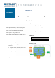
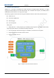
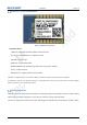
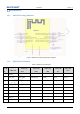
Table Of Contents
- Abstract
- Version Record
- 1. Product Introduction
- 2. Electrical Parameters
- 3. RF Parameters
- 4. Antenna Information
- 5. Production Instruction
- 6. Reference Circuit
- 7. FCC and IC Information
- 8. Module MOQ and packaging information
- 9. Sales Information and Technical Support

Datasheet [Page 3]
EMW3072
Figure Catalogue
Figure 1 EMW3072 Hardware Block and Interface ........................................................................................ 4
Figure 2 EMW3072 label picture.................................................................................................................... 5
Figure 3 Stamp Hole Packaging Dimension Diagram ..................................................................................... 6
Figure 4 EMW3072 Packaging Definition Diagram ........................................................................................ 7
Figure 5 EMW3072 Drawings ...................................................................................................................... 15
Figure 6 PCB Minimum clearance area of antenna(Unit: mm) ................................................................. 16
Figure 7 Humility Card ................................................................................................................................ 17
Figure 8 Storage Condition ........................................................................................................................... 19
Figure 9 Temperature Curve Reference ......................................................................................................... 20
Figure 10 Power Reference Circuit ............................................................................................................... 21
Figure 11 USB to UART Reference Circuit .................................................................................................. 21
Figure 12 EMW3072 External Interface Reference Design ........................................................................... 21
Figure 13 3.3V UART- 5V UART Conversion Reference Circuit .................................................................. 22
Table Catalogue
Table 1 EMW3072 pin definition ................................................................................................................... 7
Table 2 Input voltage range ............................................................................................................................ 9
Table 3 Absolute Maximum Ratings ............................................................................................................... 9
Table 4 Power Consumption Parameters ......................................................................................................... 9
Table 5 Temperature and Humidity conditions .............................................................................................. 10
Table 6 ESD Parameters ............................................................................................................................... 10
Table 7 RF Standard ......................................................................................................................................11
Table 8 IEEE 802.11b Mode CCK_11 Tx Parameters ....................................................................................11
Table 9 IEEE802.11g Mode OFDM_54 TX Performance Parameters............................................................ 12
Table 10 IEEE802.11n-HT 20MHz Mode MCS7 TX Performance ............................................................... 13
Table 12 PCB Antenna ................................................................................................................................. 15
Table 13 Module MOQ and packaging information ...................................................................................... 25