
User's Manual


Smart Machine Smart Decision
SIM7500A_User Manual_V1.00 2017-06-30
36
The maximum gain of the Main antenna gain should not exceed 3.49dBi for LTE Band 4
and 2.2dBi for LTE Band 13 considering the SAR radio. It has according to reference trace
and matching circuit testing all FCC items, and all items satisfy FCC requirements. Only
the reference trace and matching circuit is certified,antenna design must refer to it, any
other deviations require testing Class II applications as required by FCC.
The certified matching circuit as following:
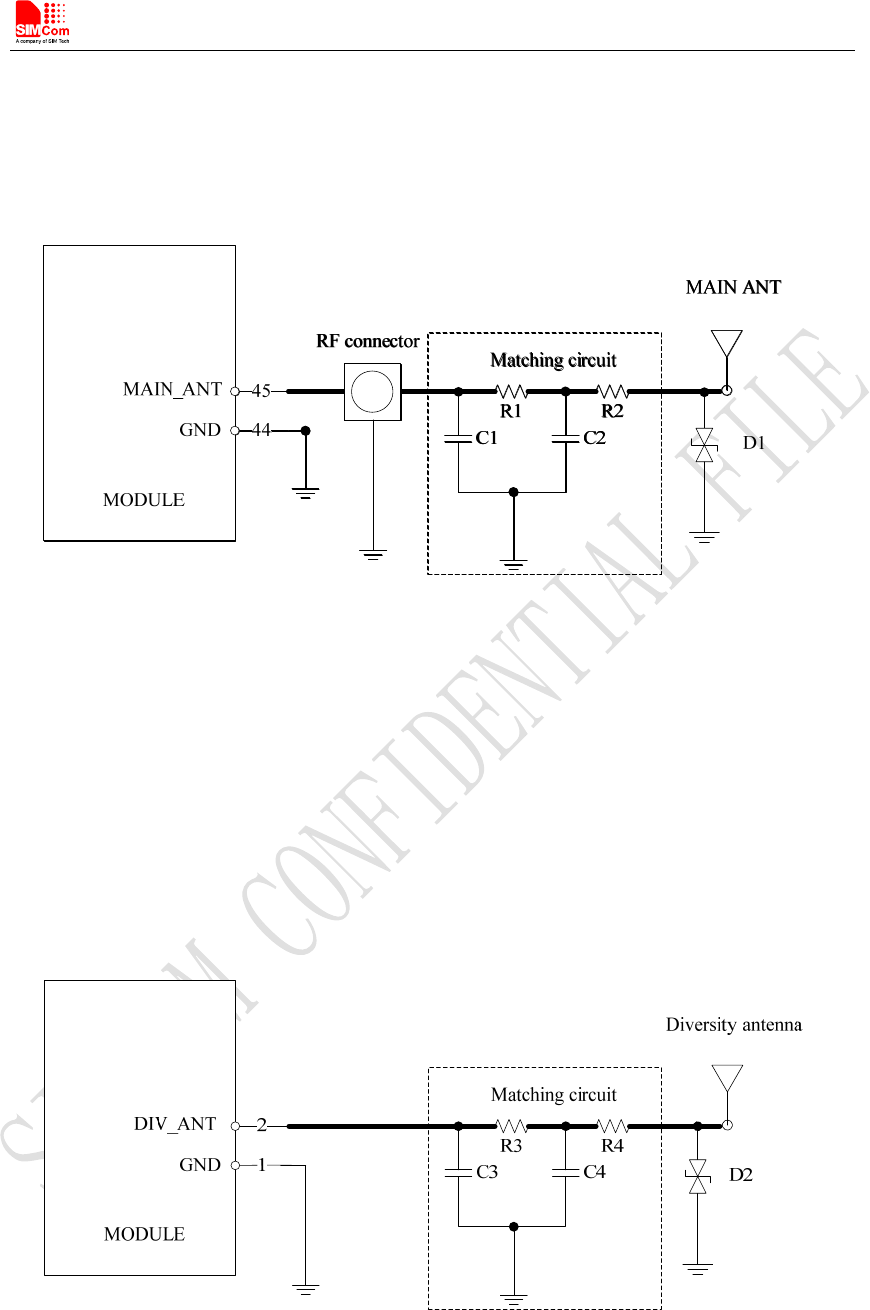
Figure 27: Antenna matching circuit (MAIN_ANT)
In above figure, the components R1,C1,C2 and R2 are used for antenna matching, the value of
components can only be achieved after the antenna tuning and usually provided by antenna vendor.
By default, the R1, R2 are 0Ω resistors, and the C1, C2 are reserved for tuning. The component D1
is a TVS for ESD protection, and it is optional for users according to application environment.
The RF test connector is used for the conducted RF performance test, and should be placed as close
as to the module’s MAIN_ANT pin. The traces impedance between Module and antenna must be
controlled in 50Ω.
Figure 28: Antenna matching circuit (DIV_ANT)
In above figure, R3, C3, C4 and R4 are used for auxiliary antenna matching. By default, the R3, R4
are 0Ωresistors, and the C3, C4 are reserved for tuning. D2 is a TVS for ESD protection, and it is