
Data Sheet


NCP7800
http://onsemi.com
10
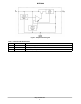
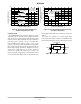
Figure 13. Worst Case Power Dissipation vs.
Ambient Temperature (TO−220)
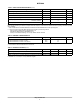
Figure 14. Input Output Differential as a Function
of Junction Temperature
, POWER DISSIPATION (W)
D
20
16
12
8.0
4.0
0
-50 -25 0 25 50 75 100 125 150
T
A
, AMBIENT TEMPERATURE (°C)
P
DIFFERENTIAL (V)
in out
, INPUT-OUTPUT VOLTAGE
0.5
0
-75 -50 -25 0 25 50 75 100
T
J
, JUNCTION TEMPERATURE (°C)
- VV
DV
O
= 2% of V
O
2.0
1.5
1.0
2.5
125
q
HS
= 0°C/W
q
HS
= 5°C/W
q
HS
= 15°C/W
No Heatsink
q
JC
= 7.5°C/W
q
JA
= 65°C/W
T
J(max)
= 150°C
I
O
= 1.0 A
I
O
= 500 mA
I
O
= 200 mA
I
O
= 20 mA
I
O
= 0 mA
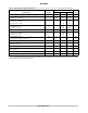
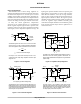
Protection Diode
The NCP7800 Series has internal low impedance (about
1 W) diode path that normally does not require protection
when used in the typical regulator applications. The path
connects between output and input and it can withstand a
peak surge current of about 5 A for a reasonable time
(several milliseconds). Normal cycling of Vin cannot
generate a current surge of this magnitude for too long time
since output capacitor discharges from output to input and
follows input voltage therefore the magnitude of reverse
current is not so high. However, when Vin is shorted or
crowbarred to ground and output cap is too large and
moreover if higher voltage option is used then the peak of
reverse current is much higher than 5 A and lasts more than
several milliseconds. In this case a damage may occur to the
regulator.
To protect the regulator the external bypass diode
connected between output and input is recommended. The
protection diode should be rated for sufficient peak current.
Figure 15. Protection Diode Placement
Input
Cin
NCP78XX
Protection Diode
Cout
Output