
Data Sheet


NCP7800
http://onsemi.com
11
DEFINITIONS
Line Regulation − The change in output voltage for a
change in the input voltage. The measurement is made under
conditions of low dissipation or by using pulse techniques
such that the average chip temperature is not significantly
affected.
Load Regulation − The change in output voltage for a
change in load current at constant chip temperature.
Maximum Power Dissipation − The maximum total
device dissipation for which the regulator will operate
within specifications.
Quiescent Current − That part of the input current that is
not delivered to the load.
Output Noise Voltage − The rms ac voltage at the output,
with constant load and no input ripple, measured over a
specified frequency range.
Long Term Stability − Output voltage stability under
accelerated life test conditions with the maximum rated
voltage listed in the devices’ electrical characteristics and
maximum power dissipation.
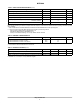
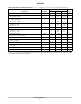
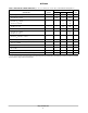
ORDERING INFORMATION
Device Nominal Voltage
Operating
Temperature Range
Package Shipping
NCP7805TG 5.0 V T
J
= 0°C to +125°C TO−220
(Pb−Free)
50 Units / Rail
NCP7808TG 8.0 V T
J
= 0°C to +125°C TO−220
(Pb−Free)
50 Units / Rail
NCP7812TG 12 V T
J
= 0°C to +125°C TO−220
(Pb−Free)
50 Units / Rail
NCP7815TG 15 V T
J
= 0°C to +125°C TO−220
(Pb−Free)
50 Units / Rail