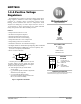
Data Sheet
Manuals
Brands
Sharp Manuals
5.0 V DC Regulators
5V 1A Linear Regulator TO220AB
1
2
3
4
5
6
7
8
9
10
NCP7800
http://onsemi.com
2
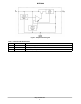
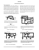
Figure 2. Simplified Block Diagram
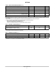
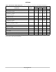
T
able 1. PIN FUNCTION DESCRIPTION
Pin No.
Pin Name
Description
1
V
in
Positive Power Supply Input.
2
GND
Power Supply Ground; Device Substrate.
3
V
out
Regulated Output V
oltage.
1
2
3
4
...
...
12