
Data Sheet
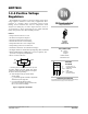


NCP7800
http://onsemi.com
7
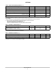
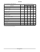
Table 8. ELECTRICAL CHARACTERISTICS (V
in
= 23 V, I
O
= 500 mA, T
J
= 0°C to 125°C, unless otherwise noted) (Note 13)
Characteristic
Symbol
NCP7815
Unit
Min Typ Max
Output Voltage (T
J
= 25°C) V
O
14.40 15 15.60 Vdc
Output Voltage (5.0 mA ≤ I
O
≤ 1.0 A, P
D
≤15 W)
17.5 Vdc ≤ V
in
≤ 30 Vdc
V
O
14.25 15 15.75
Vdc
Line Regulation (T
J
= 25°C)
17.9 Vdc ≤ V
in
≤ 30 Vdc
20 Vdc ≤ V
in
≤ 26 Vdc
Reg
line
−
−
3.3
1.8
300
150
mV
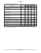
Load Regulation (T
J
= 25°C)
5.0 mA ≤ I
O
≤ 1.5 A
Reg
load
− 6.9 300
mV
Quiescent Current (T
J
= 25°C) I
B
− 3.0 8.0 mA
Quiescent Current Change
17.5 Vdc ≤ V
in
≤ 30 Vdc
5.0 mA ≤ I
O
≤ 1.0 A
DI
B
−
−
−
−
1.0
0.5
mA
Ripple Rejection (Note 14)
18.5 Vdc ≤ V
in
≤ 28.5 Vdc, f = 120 Hz
RR 54 70 − dB
Dropout Voltage (I
O
= 1.0 A, T
J
= 25°C) (Note 14) V
I
− V
O
− 2.0 − Vdc
Output Noise Voltage (T
J
= 25°C) (Note 14)
10 Hz ≤ f ≤ 100 kHz
V
n
− 6.8 −
mV/V
O
Output Resistance f = 1.0 kHz (Note 14) r
O
− 4.7 −
mW
Short Circuit Current Limit (T
J
= 25°C) (Note 14)
V
in
= 35 Vdc
I
SC
− 0.3 − A
Peak Output Current (T
J
= 25°C) (Note 14) I
max
− 2.4 − A
Average Temperature Coefficient of Output Voltage (Note 14) TCV
O
− 0.42 − mV/°C
13.Performance guaranteed over the indicated operating temperature range by design and/or characterization, production tested at
T
J
= T
A
= 25°C. Low duty cycle pulse techniques are used during testing to maintain the junction temperature as close to ambient as possible.
14.Value based on design and/or characterization.