72GF-66E SERVICE MANUAL SEJB72GF66E00 ssued 21s May 2001 DA-100W CHASSIS PAL SYSTEM COLOUR TELEVISION MODEL 72GF-66EDE/ES/GG/IT/CH In the nterests of user safety (requ red by safety regu at ons n some countr es) the set shou d restored to ts or g na cond t on and on y parts dent ca to those spec f ed shou d be used.
72GF-66E SERVICE MANUAL UPDATE LOG SHEET Technical Report No. Technical Bulletin No. Cause / Solution Part No. Page No. Application Data /Serial No. Use this page to keep any special servicing information as Technical Report (Bulletin), Technical Information, etc. If only part number changes are required, just change part number directly the part number in the Parts Listing Section. If you need more information, please refer to the Technical Report (Bulletin).
72GF-66E ELECTRICAL SPECIFICATIONS •Power Input .................... 220V-240 Volts AC 50Hz •Power Consumption Normal Operation .................................110W Stand-by Operation ..................................1W •Audio Power Output Rating (MPO) / Impedance Internal Left Speaker...................15W (MPO) Internal Right Speaker.................15W (MPO) Internal Centre Speaker..........15W (MPO) Internal Subwoofer......................20W (MPO) •Speakers Left / Right.........................
72GF-66E IMPORTANT SERVICING NOTES Only qualified service personnel are allowed to carry out maintenance and repair of this receiver. SERVICING OF HIGH VOLTAGE SYSTEM AND CRT It is important that the static charge is removed from the high voltage system when carrying out work on the receiver. This can be achieved by connecting a 10K resistor (with a suitably insulated lead) from the CRT cavity connector to the CRT ground tag. This must be carried out with the AC supply disconnected from the receiver.
72GF-66E ADJUSTMENT PROCEDURES All adjustments to this chassis, except for focus, are carried out in the service mode. • SERVICE MODE The service mode is provided to enable the engineer to correctly set up the receiver to the CRT fitted in the set. Note that these adjustments may vary from one receiver to another. To enter the service mode, carry out the following procedure. 1. Connect a test pattern to the antenna terminal. 2. Tune the receiver to this signal. 3.
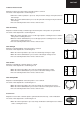
72GF-66E The following geometry adjustments can be carried out.
2GF-66E Lower Corner Correction Adjust the Lower Corner Correction so that the picture is centred. The effect of this adjustment is shown in figure 7. • When the volume up button is pressed, side pincushion changes from pincushion to barrel shape. • When the volume down button is pressed, side pincushion changes from pincushion to barrel shape. • Press the stand-by button on the remote control to store. Fig.
72GF-66E • When the volume down button is pressed the top and bottom scanning decreases and the centre scanning increases. • Press the stand-by button on the remote control to store. Vertical Shift Adjust the Vertical Shift so that the picture is centred. The effect of this adjustment is shown in figure 13. • When the volume up button is pressed, the picture moves up. • When the volume down button is pressed, the picture moves down. • Press the stand-by button on the remote control to store.
72GF-66E 4. Once this data has been set, press the standby button to store. 5. If another NVM value has to be changed, use the channel down button to select the page or position and repeat as necessary. Note: DO NOT change any NVM data, unless you have been advised to do so by a Sharp representative. If data is incorrectly changed, serious damage may occur to the receiver.
72GF-66E MOTHER UNIT PRINTED WIRING BOARD (F7293N5A). Component side. (SW2) S705 R791 R790 J344 C706 (OPC) R792 C739 (G) C719 F7294BMN5 2 R728 + JF48 FB501 R553 J134 R612 J207 2 J326 3 2 R533 R616 J178 J175 J176 J177 J174 R603 R608 D610 C619 R536 J264 JL14. (AV). R408 C648 JF50 (EW) 20 1 L603 21 C611 JF51 L605 TP601 21 20 J306 R611A L612 4 F601 J316 6 JL1 R614 (YC) Page 11 L611 3 D516 6 D608 7 C641 C618 5 D604 C642 JL2.
72GF-66E .A 1 4 C356 (FV). 3 9 C376 6 (SB) 12 6 J199 12 J275 C204 2 TU AGC 24 11 25 26 27 28 29 30 1 JL19 J278 23 J131 R233 + 22 J130 J301 CL (L2) TH201 21 J225 C206 C211 R232 TP201 20 3 DA AS L203 C218 19 (SA) 1 C215 C426 4 C209 R234 J274 R436 FB303 R424 B+ J260 1 (FV) C422 1 + 2 18 J170 C329 C210 JF19 C325 C324 C323 J169 5 1 J271 C821 AV J348 J349 J347 R420 R425 33V IC203 J252 R418 FB302 C415 JL12.
72GF-66E TH201 Y 32 31 30 JF20 C429 Q209 J278 29 R1804 D1809 R1806 C1802 R1817 R1823 R1824 R1818 C1803 R1834 R1031 R2405 R1029 52 J87 C521 D411 C416 R428 J183 R511 R516 28 27 26 25 24 12 23 22 21 R502 R512 J178 R533 J179 C644 R530 + D601 C515 R403 D422 K R457 C401 R413 R40 C411 C414 R414 R450 R434 R406 C403 R404 C405 R415 C410 C409 20 19 18 Q404 K R412 D415 D414 C406 R405 C402 C412 R417 D405 R410 R462 Q405 C404 J266 R416 Q406 J265 D4
72GF-66E MOTHER UNIT PRINTED WIRING BOARD (F7293N5A). Copper side.
72GF-66E D5410 C853 C877 R856 B 1 2 3 4 C895 (MO) C1613 9 Q1603 10 12 11 13 L317 R449 2 4 L318 (CC) 1 (J) F7306BMN0 1 2 3 4 5 14 6 B 7 8 9 10 (SVM) D5403 C5405 R892 6 JF8 E 1 CN4 J401 Q5412 C Q1604 35 3 X R1622 Q5410 (B) . F7269BMN3 7 1 (FV) R5434 E E C E 4 0 R5432 C1609 R1623 E C FRONT A/V UNIT PRINTED WIRING BOARD. (F7306N0B). Component side.
72GF-66E CRT MODULE UNIT PRINTED WIRING BOARD (F7269N3). Copper side. (B) Q1604 Q1603 14 13 C874 C889 C859 + Q853 R855 Q855 C861 J7 R860 R863 (K) C881 D869 D868 J18 J8 J1 C871 R872 (RT) C887 + C893 R5440 Q860 R874 R882 Q861 R885 J10 JF7 C865 R881 R866 D867 R886 (Q) 1 R876 J15 C5425 J5 Q859 FB852 C885 R852 C1608 J17 C856 Q5415 1 IC852 C884 R884 B .
GND DYN.INPUT .
72GF-66E DIGITAL MODULE UNIT PRINTED WIRING BOARDS (F7295NOA). 16 16 C6014 12 1 IC6002 Comp.
72GF-66E POWER SWITCH UNIT PRINTED WIRING BOARDSM (F7305N0B). Copper side.
72GF-66E AUDIO AMPLIFIER UNIT PRINTED WIRING BOARDS (F7304N0B).
72GF-66E MOTHER UNIT (F7293N5A) PWB PARTS LOCATION TABLES. Component Side.
72GF-66E MOTHER UNIT (F7293N5A) PWB PARTS LOCATION TABLES. Component Side.
72GF-66E MOTHER UNIT (F7293N5A) PWB PARTS LOCATION TABLES. Copper Side.
72GF-66E MOTHER UNIT (F7293N5A) PWB PARTS LOCATION TABLES. Copper Side.
72GF-66E CRT MODULE UNIT PWB (F7269N3) PARTS LOCATION TABLES. Component Side.
72GF-66E FRONT A/V UNIT PWB (F7306N0B) PARTS LOCATION TABLES. Component Side. Ref No (CC) Copper side (FV) (J) Xum Yum Ref No 60426 14224 C336 49504 14224 C337 82270 11734 (SS) 32232 CN4 J401 L317 L318 R449 DINAMIC FOCUS UNIT PWB (F7271N3) PARTS LOCATION TABLES. C428 79984 40005 C429 63500 40005 JF1 74955 18084 JF2 21564 20574 JF3 50266 22860 R316 R317 14224 Component Side.
72GF-66E DIGITAL MODULE UNIT (F7295N0B) PWB PARTS LOCATION TABLES. Component Side.
72GF-66E DESCRIPTION OF SCHEMATIC DIAGRAM SAFETY NOTE: 1. DISCONNECT THE AC PLUG FROM THE AC OUTLET BEFORE REPLACING PARTS. 2. SEMICONDUCTOR HEAT SINKS SHOULD BE REGARDED AS POTENTIAL SHOCK HAZARDS WHEN THE CHASSIS IS OPERATING. IMPORTANT SAFETY NOTE: NOTE: 1. The unit of resistance «ohm»is omitted (K=1000 ohms. M= Megaohm). 2. All resistors are 1/8 watt. unless otherwise noted. 3. All capacitors are mF, unless otherwise noted (P= mmF). 4. The capacitor with Part No.
D728 C5V1 EX0545 D727 DX0551 R762 220 (TQ) 1uF (16V) R768 220 (TQ) C737 470nF 16V TV1CF474Z* C749 R763 100 (1/2W) XZ0224 IC708 FX0111 10K R767 C702 47nF 400V FZ0173 JF53 FB702 LN0037 B 7 Q701 TX0198 S5F10N80 R714 560K 1/2W R713 560K 1/2W D704 DX0555 RF2005 D702 DX0555 RF2005 L702 C710 47nF (500V) DE472Z R787 47K R735 470K R739 47K CF701 C0121 C725 4.
D601 DX0551 C606 68nF (HB) Q703 TX0151 2SD2391Q R603 330 Q702 TX0182 2PD602 R720 10K R719 220 D713 DX0551 R634 220 C738 56pF +5V C713 100nF D619 DX551 2n2 (HB) C640 D716 EX0411 6V8 R619B 560 2W Q602 TX0192 KSC2500 D612 DX0519 1N5819 L609 1.
Pag 28 2 +5V 3 R1032 27K 1686BM 10R272L C1001 AV2 R528 100K C1005 100nF +3.3V R1025 8K2 R308 100 1 OPC A0 A1 A2 A3 A4 A5 A6 A7 A8 A9 VDD VSS A10 A11 A12 A13 A14 R1024 8K2 C1018 100nF SELFI BG/L L/L' RESOUT ROT OUT RES2OUT HOUT P0H.
V OUT GN0441 (MO) C528 10uF (100V) R435 1K R450 22 D403 7V5 EX0549 D421 4V7 EX0544 R408 75 (1/4W) 04 551 R549 27K 16 G +13V 3 Q405 2SA1037 R409 75 1% R410 22K D420 C5V6 EX0546 D411 C5V6 EX0546 2 +13V C509 220uF (25V) C506 100nF R434 1K C408 10nF L E/W 1 C521 1nF 14 R548 6K8 18 R535 6K8 C510 100nF +5V -13V 4 D416 C6V2 EX0547 R460 18K 1% C507 4.7nF (HB) C505 100nF -13V AVCLOCK 12 C524 100nF 17 CIN FS 15 AL SERVICIO 11 C511 2.
72GF-66E SCHEMATIC DIAGRAM OF CRT MODULE UNIT (F7269N3), 00 Version.
72GF-66E SCHEMATIC DIAGRAM OF CRT MODULE UNIT (F7269N3), 00 Version. IC850 TDA6111Q R865 3K3 9 8 9 7 8 6 7 5 H.V. 27.
A B 5 6 1 5 4 3 2 6 7 C337 10nF Digitally signed by Castillo, Fco. cn=Castillo, Fco., ou=SEES, o=Engineering Dept., c=ES Date: 2001.05.04 15:12:13 +01'00' Reason: I have reviewed this document APROBADO R317 390 2 1 23-02-2000 72GF66E FECHA MODELO Front A / V NOMBRE (SS) GN0341 2 3 1 2 1 (CC) GN0241 R449 75 (1/4W) ELECTRONICA ESPANA S.A. SHARP A-4 ESCALA Q P W B F 7 3 0 6 B M N 0 A CODIGO (FV) GN0241 1nF 1nF L318 3.
C1602 470pF 2Kv R1603 100K (3W) R1608 1K Q1602 BC547 TX0142BM 100K (3W) R1604 NZ0575BM T1602 C1603 1000pF 2Kv 3 2 G2 1 FOC IN R1625 3K3 180 (1W) R1605 R1607 10K D1606 DX0045 D1602 DX0045 Q1601 2SC5022 R1601 33K 1/2 W 10K R1606 C1612 220uF (25V) R1609 150K C1605 3.
72GF-66E SCHEMATIC DIAGRAM OF DIGITAL MODULE UNIT (F7295N0A), 00 Version. C6006 10uF (16V) C6033 10nF C6007 1n5 C6031 3.3pF L6001 3.
72GF-66E SCHEMATIC DIAGRAM OF DIGITAL MODULE UNIT (F7295N0A), 00 Version. BM C6019 15nF RES PWM2 C6018 15nF +5V GM C6020 15nF C6014 3.
1 2 3 4 38 5 6 Digitally signed by Castillo, Fco. cn=Castillo, Fco., ou=SEES, o=Engineering Dept., c=ES Date: 2001.05.04 15:07:42 +01'00' Reason: I have reviewed this document NOMBRE Digitally signed by Castillo, Fco. cn=Castillo, Fco., ou=SEES, o=Engineering Dept., c=ES Date: 2001.05.
5 6 1 (RC) GN0341 Digitally signed by Castillo, Fco. cn=Castillo, Fco., ou=SEES, o=Engineering Dept., c=ES Date: 2001.05.04 15:08:37 +01'00' Reason: I have reviewed this document 2 Digitally signed by Adolfo Fernandez cn=Adolfo Fernandez, ou=CAD GLOBAL NETWORK, o=SHARP, c=ES Date: 2001.05.04 13:22:02 Z Reason: This document is ready for approval 3 VERIFICADO R6702 120K 1/2W C REALIZADO (A) GN0207 R6701 120K 1/2W F6701 FS-C3226 (SW1) GN0341 Digitally signed by Castillo, Fco. cn=Castillo, Fco.
A B 5 6 Digitally signed by Castillo, Fco. cn=Castillo, Fco., ou=SEES, o=Engineering Dept., c=ES Date: 2001.05.04 15:11:55 +01'00' Reason: I have reviewed this document VERIFICADO R317 390 1 5 4 3 2 6 7 C337 10nF Digitally signed by Castillo, Fco. cn=Castillo, Fco., ou=SEES, o=Engineering Dept., c=ES Date: 2001.05.
72GF-66E STEREO LED FLASHING CODES. If the TV set does not work and the stereo led is flashing, follow the sequence according to the information below, as a guide to fault finding. 1. Unable to read or write into NVM: 66% ON, 33% OFF twice and OFF for a second. On Off 2. MSP failure: 66% ON, 33% OFF for three times and OFF for a second. On Off 3. VPC failure: 66% ON, 33% OFF for four times and OFF for a second. On Off 4. SAA4956 failure: 66% ON, 33% OFF for six times and OFF for a second. 5.
72GF-66E BLOCK DIAGRAM A B C SF 201 SAW TH 201 FM AUDIO IF IF SF 202 SAW TUNER IC 201 CVBS TDA 4470 1 I2C SF 203 SAW 21 PINS RGB RGB 21 PINS V AV-2 MAIN POWER M 6701 IR DETECTOR + CH - + 21 PINS VOL - V AV-1 DIGITAL MODULE AV-FRONT S 6701 IC 401 S-VIDEO HEF 4053 SWITCH V IC 6001 VPC 3230 I2C VIDEO PROCESSOR 2 IC 702 IC 704 Micro Proc. ADG COIL Micro Proc. COMUNICATION ON/ST-BY POWER ST-BY CONTROL IC 703 +5V PTC POR 701 IC 701 Micro Proc.
72GF-66E BLOCK DIAGRAM D E I2C C CENTRAL SPEAKER MODULE 7 +16V 3 + IC1302 - 6 CENTER 4 IC 305 -16V MSP 3410 D 7 +16V PERIPHERICS AUDIO L/R 3 1 6 AUDIO OUT L Q 304 4 2 + IC 301 - -16V Q 302 AUDIO PROTECTOR Q 303 7 +16V 3 + IC 302 - 6 AUDIO OUT R 4 2 -16V Q 305 Q 306 MUTE I2C I2C I2C MODULE 7295 IC 304 IC 6002 IC 6003 SDA 9400 DDP 3310-E4 DIGITAL SCAN CONVERTER + PIP PROCESSOR HEADPHONE CONECTOR DISPLAY DEFLECTION PROCESSOR +13V 2 IC 502 V.
72GF-66E PARTS LISTING REPLACEMENT PARTS Replacement parts which have special safety characteristics are identified in this manual. Electrical components having such features are identified by ! in the Replacement Part List. The use of a substitute replacement part which does not have the same safety characteristics as the factory recommended is not permitted. Replacement parts not shown in this service manual may create shock fire, or other hazards.
72GF-66E REF No. PARTS D D D D D D D D D D D D D D D D D D D D D D D D D D D D D D D D D D D D D D D D D D D D D D D D D D D D D D D D D D DESCRIPTION * SN CODE EX CODE REF No.
72GF-66E REF No. PARTS DESCRIPTION * SN CODE EX CODE REF No.
72GF-66E ! REF No. PARTS DESCRIPTION * SN CODE EX CODE REF No.
72GF-66E REF No. PARTS DESCRIPTION * SN CODE EX CODE REF No.
72GF-66E R R R R R R R R R R R R R R R R R R R R R R R R R R R R R R R R R R R R R R R R ! ! 1029 1030 1031 1032 1035 1036 1037 1038 1039 1040 1041 1042 1043 1044 1045 1046 1047 1048 1049 1050 1051 1052 1053 1054 1055 1056 1058 1059 2401 2402 2403 2404 2405 2406 2407 2408 2409 2410 2411 2412 IC 1002 (A) (AV) (CN2) (CN1) (F) (FV) (G) (PW) (RG) (SP) (YA) (YB) (YC) F 0701 FB 0302 FB 0303 FB 0501 FB 0603 FB 0701 FB 0702 FB 0703 FB 0705 FB 1001 J 0002 J 0012 J 0013 J 0014 J 0061 J 0065 J 0072 J 0075 J 0098
72GF-66E ! REF No. PARTS DESCRIPTION * SN CODE EX CODE REF No.
72GF-66E REF No. PARTS DESCRIPTION * SN CODE EX CODE REF No.
72GF-66E DESCRIPTION * SN CODE EX CODE REF No.
72GF-66E REF No.
72GF-66E REF No. PARTS DESCRIPTION * EX CODE REF No.
72GF-66E 1 1.1 1.2 1.3 1.5 1.6 1.4 1.7 1.
72GF-66E No part of this publication may be reproduced, stored in a retrieval system, or transmitted in any form or by any means, electronic, mechanical, photocopying, recording, or otherwise, without prior written permission of the publisher. SHARP ELECTRONICA ESPAÑA S.A. TV Division Engineering Dept.