CD-PC1881V SERVICE MANUAL No. S0961CDPC1881 CD-PC1881V CD-PC1881V Video CD Mini System consisting of CD-PC1881V (main unit), CP-C881 (front speakers), CP-SW881 (sub woofer), GBOXS0026AWM1 (center speaker) and GBOXS0027AWM1 (surround speakers). NTSC/PAL Manufactured under license from Dolby Laboratories Licensing Corporation. DOLBY, the double-D symbol and “PRO LOGIC” are trademarks of Dolby Laboratories Licensing Corporation.
CD-PC1881V SAFETY PRECAUTION FOR SERVICE MANUAL Precaution to be taken when replacing and servicing the Laser Pickup. The AEL (Accessible Emission Level) of Laser Power Output for this model is specified to be lower than Class I Requirements. However, the following precautions must be observed during servicing to protect your eyes against exposure to the Laser beam.
CD-PC1881V FOR A COMPLETE DESCRIPTION OF THE OPERATION OF THIS UNIT, PLEASE REFER TO THE OPERATION MANUAL. SPECIFICATIONS CD-PC1881V General Power source: Power consumption: Dimensions: Weight: Tuner section AC 110/127/220/230-240 V, 50/60 Hz 140 W Width; 270 mm (10-5/8") Height; 300 mm (11-13/16") Depth; 362 mm (14-1/4") 8.1 kg (17.7 lbs.) Frequency range: Front speakers; MPO; 176 W(88 W + 88 W) (10 % T.H.D.) RMS; 80 W (40 W + 40 W) (10 % T.H.D.) RMS; 72 W (36 W + 36 W) (0.9 % T.H.D.
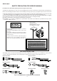
CD-PC1881V NAMES OF PARTS CD-PC1881V ■ Front panel 1 1. Disc Number Selector Buttons 2. Disc Tray 3. Multi Indicator 4. Disc Skip Button 5. Open/Close Button 6. Dolby Pro Logic Indicator 7. Extra Bass Indicator 8. FM Stereo Mode Indicator 9. FM Stereo Indicator 10. (VCD/CD) Play Indicator 11. (VCD/CD) Pause Indicator 12. (VCD/CD) Repeat Indicator 13. (VCD/CD) Disc Number Indicators 14. (VCD/CD/TUNER) Memory Indicator 15. Timer Play Indicator 16. Timer Record Indicator 17.
CD-PC1881V ■ Rear panel 1. Video Output Socket 2. AC Power Lead 3. AM Aerial Terminal 4. Aerial Earth Terminal 5. FM 75 Ohms Aerial Terminal 6. Video/Auxiliary (Audio Signal) Input Sockets 7. AC Voltage Selector 8. Surround Speaker Terminals 9. Centre Speaker Terminals 10. Front Speaker Terminals 11. Sub Woofer Terminals 3 4 1 5 6 2 7 8 9 10 11 CP-C881 ■ Front speaker 1 2 1. Super Tweeter 2. Tweeter 3. Woofer 4. Bass Reflex Duct 5. Speaker Wire 3 4 5 GBOXS0026AWM1 ■ Center speaker 6.
CD-PC1881V ■ Remote control 1. Remote Control Transmitter LED 1 2. On/Stand-by Button 3. Surround Level Buttons 4. Centre Level Buttons 5. Dolby Pro Logic Button 6. Centre Mode Button 7. Test Tone Button 3 4 5 6 8. (VCD/CD) Direct Search Buttons 9. (VCD) On Screen Display On/Off Button 10. (VCD) PAL/NTSC Select Button 11. (VCD) Book Mark Button 12. (VCD) Digest/Time Search Button 13. (VCD/CD) Audio Mode Button 14. (VCD) VCD Auto/On Button 15. (VCD) Playback Control Auto/Off Button 16.
15 15 Replace the batteries if the operating distance is reduced or if the operation becomes erratic. Periodically clean the transmitter LED on the remote control and the sensor on the main unit with a soft cloth. Exposing the sensor on the main unit to strong light may interfere with operation. Change the lighting or the direction of the unit. Keep the remote control away from moisture, excessive heat, shock, and vibrations. Notes concerning use: 0.
CD-PC1881V DISASSEMBLY Top Cabinet Front Panel (A1)x2 ø3x12mm Caution on Disassembly Follow the below-mentioned notes when disassembling the unit and reassembling it, to keep it safe and ensure excellent performance: 1. Take cassette tape and compact disc out of the unit. 2. Be sure to remove the power supply plug from the wall outlet before starting to disassemble the unit. 3. Take off nylon bands or wire holders where they need to be removed when disassembling the unit.
CD-PC1881V (M1) x1 ø3 x10mm Front Panel Display PWB (M2) x1 (G1)x2 Washer (H3)x2 (H4)x4 1 Push 1 Push 2 Pull POWER PWB Turntable (G2)x1 (H3)x2 (G3)x1 Headphoens PWB Power PWB Disc Tray (G4)x1 (N1) x1 ø3 x10mm (H1)x4 ø3x10mm (G6)x1 (G5)x1 (H2)x2 ø3x10mm ø3x6mm Main PWB (N2) x1 Figure 9-1 (N1) x1 ø3 x10mm (L2)x1 Switch PWB CD Player Unit Figure 9-3 (K3)x1 (K1)x2 ø3x10mm (N2) x1 Display PWB (P1) x1 ø3 x10mm Front Panel (K1)x10 ø3x10mm (K2)x1 CD Video PWB (P2) x2 Headphones PWB Ma
CD-PC1881V CP-C881 STEP 1 REMOVAL PROCEDURE Front Speaker 1. Front Panel ............ 2. Tip .......................... 3. Screw ..................... 4. Screw ..................... 5. Screw ..................... FIGURE (A1) x1 (A2) x2 (A3) x2 (A4) x2 (A5) x4 Speaker Box Super Tweeter 10-1 (A3)x2 ø3x10mm (A2)x2 (A4)x2 ø3x10mm (A5)x4 ø4x14mm Tweeter Woofer Front Panel (A1)x1 Drive should be pried away from Speaker Box.
CD-PC1881V REMOVING AND REINSTALLING THE MAIN PARTS CD MECHANISM SECTION Perform steps 1, 2, 3 and 14-16 of the disassembly method to remove the CD mechanism. How to remove the T/T up/down loading motor (See Fig. 11-1) 1. Remove the screws (A1) x 2 pcs., to remove the T/T up/ down loading motor. T/T Up/Down Loading Motor Motor PWB (A1) x2 ø2.6 x5mm Figure 11-1 How to remove the pickup (See Fig. 11-2) 1. Remove the screws (B1) x 2 pcs., to remove the shaft (B2)x 1 pc. 2.
CD-PC1881V ADJUSTMENT MECHANISM SECTION TUNER SECTION • Driving Force Check fL: Low-range frequency fH: High-renge frequency • AM IF/RF Signal generator: 400 Hz, 30%, AM modulated Torque Meter Specified Value Play: TW-2412 Tape 1: Over 80 g Tape 2: Over 80 g • Torque Check Torque Meter Specified Value Tape 1 Tape 2 Play: TW-2111 30 to 60 g. cm Fast forward: TW-2231 — 30 to 60 g.cm 60 to 120 g.cm Rewind: TW-2231 — 60 to 120 g.
CD-PC1881V TEST MODE • Setting the test mode Any one of test mode can be set by pressing several keys as follows. + < > + TEST: CD operation test • TEST mode Function — CD test mode Setting of TEST mode Indication of CD TST mode (Fig. 13-1) IL is not performed. OPEN/CLOSE operation is manual operation. The pickup can be moved by using the ( LASER ON Tracking on the spot. SERVO OFF PLAY key input ) or ( ) key. Tracking on the spot.
CD-PC1881V EXPLANATION OF DOLBY SURROUND PRO LOGIC AND EVALUATION METHOD Outline • In the normal mode of Pro Logic ON mode the amplifiers for C-ch and S-ch are in operative state, so that the SP output appears. • In the Phantom mode of Pro Logic ON mode the amplifier for C-ch is in MUTE state, so that the SP output is cut. The amplifier for S-ch (surround) is in operative state, so that the SP output appears • Namely, two speakers are connected in parallel to one amplifier.
SOLM2 SOLENOID SW1 OPEN/CLOSE M3 T/T UP/DOWN LOADING MOTOR SW3 DISC NUMBER SW2 MECHA UP CD-PC1881V M TO MAIN SECTION TO MAIN SECTION 87654321 +B1 GND (D) MECHA UP GND (D) DISK NO. OPEN/CLOSE GND (D) M– M+ SOLSOL+ CNS10 10 9 1 2 3 4 5 6 CNP11 +B1 +B5 CNP10 10 9 QV4 JKV1 VIDEO OUT 87654321 R L 1 6 20 VDD 36 DQ12 1 DQ8 UCAS 28 LCAS 29 A8 A3 A4 DQ0 39 DQ15 WE RAS A0 ~ ICV4 VIDEO OPERATION AMP.
CD-PC1881V SO301 ANTENNA TERMINAL FM IF FE301 FM FRONT END 1 1 +B4 CF302 3 AM IF 2 3 1 VT AM CF352 +B4 2 OUT 4 5 8 9 IN GND VCC IC303 LA1832 FM/AM IF MPX.
CD-PC1881V FL701 FL DISPLAY Q702 Q703 M 1 2 3 4 ~ 15 16 ~ 25 26 ~ 28 29 ~ 36 37 38 39 MM1 APE MOTOR Q705 Q706 Q707 TO CD VIDEO SECTION S22/DIST4 S21/DIST3 S20/DIST2 S19/DIST1 S18/DIST0 S17 S16 S15 S14 S13 S12 S11 VLOAD S10 SPRLY MBUSY POWER 81 82 83 84 S5 85 S4 86 S3 87 S2 88 S1 89 G11 90 G10 91 G9 92 G8 93 G7 94 G6 95 G5 96 G4 97 G3 98 99 100 UNSWITCH +B7 MEMORY +B4 BACK UP M 30 29 28 27 26 25 24 23 22 21 20 19 18 17 16 15 14 13 12 11 10 9 8 7 6 5 4 3 2 1 +B5 PHM1 KEY SW701~SW721 SW722~SW
CD-PC1881V TO CD VIDEO PWB P27 12-C CNP11 TO TUNER PWB P21 12-A CNP303 TO DECK SECTION P20 2-A CNS303 1 2 3 4 5 6 CNS11 1 2 3 4 5 6 R-CH A_GND L-CH D_GND 7.
CD-PC1881V WB CNS11 BI401 FM SIGNAL C448 2.2/50 R401 27K R404 1.8K C462 390P R402 27K C463 390P C464 390P R-CH C465 0.001 +B +B C460 0.022 +B R483 100K 5 6 C477 100P C478 0.082 (ML) 4 R480 1.5K C479 10/50 R627 100 R424 220K C609 100P 8 R611 560 C603 47/25 C604 47/25 R612 560 C606 100P 2 3 1 5 6 7 R617 C611 R621 1K 10/50 2.7K R616 1K 4 C657 270P R654 68K C659 0.0027 R653 12K C653 0.0027 D651 DS1SS133 R655 56K C655 0.0068 R656 470K CNP501 OPE AMP.
CD-PC1881V TO MAIN SECTION P18 3-A 16 MAIN PWB-A1(2/2) C652 0.01 M_GND A_12V D_GND 15 14 17 MECHANISM CHASSIS BOTTOM CHASSIS +B TAPE_L BIAS 21 12 A_GND 19 REC_L REC_R T1/T2 TAPE_R A REC_MUTE 11 13 18 20 +B +B R164 4.7K D101 DS1SS133 R181 220K D102 DS1SS133 B C152 47/25 Q126 KRC104 M 0V 1 2 3 0V 11.6V R162 47K 11.6V R168 12 0V Q128 KTC3203 Y R166 47K 0V 11.7V R158 220 R167 100K R160 150 (1/2W) L104 330µH 0V 0V C151 0.027 (ML) C150 0.
CD-PC1881V TUNER PWB-G FM SIGNAL CNP303 D GND 1 DO 2 CLK 3 CE 4 DI 5 A+12V 6 A GND 7 L 8 R 9 AM SIGNAL +B C396 100/10 R358 8.2K 24 C350 AM OSC OUT FM IF IN 1 R351 5.6K VR351 10K(B) C342 0.022 IC303 LA1832 FM IF DET./ FM MPX./AM IF Q371 KTA1266 GR R387 22K ZD352 DZ3.9BSB D351 DS1SS133 D352 DS1SS133 C391 47/16 R383 5.6K R391 Q360 390 KTA1266 GR 0.022 C352 10/16 C351 0.022 3 C385 0.
CD-PC1881V +B A F F F S22 S21 S20 S19 S18 S17 S16 S15 S14 S13 S12 S11 S10 S09 S08 S07 S06 S05 S04 S03 S02 S01 G11 G10 G09 G08 G07 G06 G05 FL701 FL DISPLAY TO POWER PWB P24 1-F CNP806 R701 100K R702 100K Q707 KTC3199 GR R703 100K C702 1/50 R789 1K R728 1K R729 1K 81 82 83 84 85 86 87 88 89 90 91 92 93 94 95 96 80 S10 1 +B D722 DS1SS133 +B R790 D721 33 DS1SS133 C721 47/50 S8 S7 S6 S5 S4 S3 S2 S1 G11 G10 G9 G8 G7 G6 G5 4 Q706 KTC3199 GR MDCK 3 MBUSY 4 CNS806 UN SW_5V 1 C Q705 KTC3199 GR
CD-PC1881V +B R788 1K IC702 LED DRIVER OUTPUT R781 10K REMARK FUNCTION COLOUR F F G08 G07 G06 G05 G04 G03 G02 G01 F C716 47/16 C717 0.
CD-PC1881V A IC902 STK40724 POWER AMP. Q904 KTC3199 GR R908 68K C905 220P R906 10K R904 68K C906 1/50 + C912 100/50 R916 1K R917 R918 56K 470 C917 47/50 15 16 17 18 C923 47P C918 47/50 Ch3 Out 19 C926 47P 20 R964 4.7K 14 C915 47P C916 15P R965 4.7K C929 15P R927 R930 R931 470 56K 1K R961 39K C925 47/50 13 C924 15P 12 R924 1K 11 R922 R921 470 22K 10 R923 56K Ch2 Out 9 C911 100/50 R913 100 Fusible C934 0.1(ML) C935 0.1(ML) R909 1K C908 0.001 C936 0.1(ML) C937 0.
CD-PC1881V R969 120(1/2W) 2 Q907 KRC107 M 1 3 C979 10/50 R966 15K 2 1 1 2 2 M M901 FAN MOTOR R968 1K R967 68K R964 4.7K D909 1SS133 RL901 2 1 C978 47/50 D903 1SS133 65 K 1 CNP804 CNS800 CNP800 CNS804 M902 FAN MOTOR M Q905 KTC3199 GR F903 T3.15A L 250V RL902 F901 T3.15A L 250V C936 0.1(ML) C937 0.1(ML) F902 T3.15A L 250V C987 0.1(ML) C940 0.1(ML) D908 1SS133 R940 4.7 R937 4.7 3 2 1 – 4 3 1 2 + IC951 LA4451 POWER AMP.
CD-PC1881V C2 0.01 C32 0.01 C31 220/4 C30 0.1 +B C1 LASER 47/10 DRIVER Q1 KTA1504 GR R1 12 R2 1K C34 0.33/50 C15 0.01 C33 0.47/50 +B A C3 1/50 R46 560 R20 1K 2200P R22 820 R21 1.5K + SLOF S.Q.R + - - 39 38 R27 39K VREF 12 C17 0.001 R30 6.8K R33 1.2K R32 10K R34 1K 35 34 33 5 6 2 9 3 0 3 1 32 R36 220K 7 R35 220K C12 0.
CD-PC1881V CD VIDEO PWB-B (1/2) +B R41 47K R57 1K R58 1K R59 1K 3 14 CLV1 5 V/P 11 IC2 LC78631E SERVO/SIGNAL CONTROL 1 7 TEST3 1 8 P4 19 HFL 20 TES 21 PCK RV64 8.2K RV66 8.2K RVSS 5 5 XVDD 5 4 XOUT 52 XVSS 5 1 RV65 8.2K LVSS 5 0 LCHN 4 9 LCHP 4 8 38 P0/DFCK 39 P1/DFIN CV27 560P LVDD 4 7 MUTEL 4 6 C2F 4 5 CONT1 DACKO DFLRO LRCKO P5 SLDEMPH_B JPSLD+ JP+ VDD CV34 RV76 10/16 2.2K RV72 10K 5 CV28 180P CV29 180P 3 RV69 6.8K RV73 10K 2 R68 1K + 8 IC4 CV32 0.
CD-PC1881V B P27 12 - E TO CD SECTION A 10 13 12 11 4 9 5 19 C2PO LRCK BCLK DATAD +7V VOLTAGE REGULATOR QV1 UPC29M33 T +12V(A) +B QV4 KTA1298 Y RV84 4.7K +B CV1 47/6.3 CV3 0.22 +B GND(D) DV5 KDS193 RV85 10K QV2 KTA1298 Y +B RV1 10K GND(A) RV2 4.7K DV4 KDS193 2 QV3 KRC104 S 3 1 +12V(A) C RV16 1.2K RV17 1.2K RV6 1K CV4 47/6.3 GND(D) AUDSW SDATA SCK STROBE KEYCON RV10 1K RV9 1K RV8 1K RV7 1K TEST POINT GND(A) RV18 1K 18 CV2 0.
CD-PC1881V CD VIDEO PWB-B (2/2) VIDEO SIGNAL +B +B 1 CV17 0.01 CV40 22/6.3 CV41 4.7/25 7 8 RV63 150 1 2 RV96 33K CNSV3B 2 5 6 1 2 1 2 CNPV4 3 RV62 150 CNSV3A 4 CV39 100/10 CNPV3 ICV4 VIDEO OPERATION AMP. NJM2267M RV95 6.8K JKV1 VIDEO OUT 1 2 CV18 100/10 DV1 1SS133 RV61 100K CV15 4.7/25 JACK PWB-G DV2 1SS133 CHASIS GND RV60 100 +B HSYNC NSYNC CSYNC VCLK CV24 0.022 CV21 0.022 CV20 0.022 CV10 47/6.3 +B +B CV12 0.022 CV23 47/6.
CD-PC1881V VOLTAGE IC1 PIN NO. 1 2 3 4 5 6 7 8 9 10 11 12 13 14 15 16 17 18 19 20 21 22 23 24 25 26 27 28 29 30 31 32 33 34 35 36 37 38 39 40 41 42 43 44 45 46 47 48 49 50 51 52 53 54 55 56 57 58 59 60 61 62 63 64 VOLTAGE 2.5V 2.5V 2.5V 2.5V 2.5V 2.5V 2.5V 2.5V 2.5V 2.5V 2.5V 2.5V 2.5V 2.5V 2.5V 2.5V 2.5V 2.5V 2.5V 2.5V 2.5V 0V 2.5V 2.5V 2.5V 2.5V 2.5V 2.5V 2.5V 2.3V 2.3V 0V 0V 5.0V 5.0V 0V 0V 5.0V 0V 0V 1.6V 2.4V 2.4V 2.4V 0V 2.5V 2.5V 0V 0V 2.4V 4.6V 4.6V 0V 0V 5.0V 5.0V 2.5V 2.5V 1.0V 1.0V 2.2V 4.
CD-PC1881V SO301 ANTENNA TERMINAL FM 75 Ohms GND AM A D304 X352 C381 C392 R372 IC302 R371 C387 C380 R376 VD301 C385 C386 R336 R344 C341 R398 B C E C331 C335 C337 C384 Q360 R323 L353 R358 R385 C351 CF302 C342 CF352 C352 T351 B C E C395 ZD351 TO MAIN PWB CNS303 P32 1 - E R367 1 2 3 4 5 6 7 8 9 C375 R368 D353 R363 CNP303 C355 R354 R353 C399 R364 C396 R365 G R362 Q353 Q354 R392 C354 C356 C370 CF351 R361 B C E Q361 R393 C372 C371 L352 R352 C398 X351 C373
CD-PC1881V JK601 HEADPHONES TO DISPLAY PWB P33 7-E C621 CNP701 TO TAPE MECHANISM PWB P35 10-C TO TAPE MECHANISM PWB P35 11-C A CNS101 CNS102 HEADPHONES PWB-A4 FFC701 1 25 R620 R619 R442 R441 C437 R443 C438 C503 C519 R428 R427 R426 R434 C428 R622 R616 C612 R674 C656 D652 R652 R658 R651 C651 B C E E C B R623 R607 Q601 E C B C615 B C E Q602 WH BK WH BK WH RD MAIN PWB-A1 CNS11 R-CH L-CH R-CH L-CH VIDEO VIDEO 2 IN 1 IN JK401 CNP11 TO CD VIDEO PWB P37 7-E 1 2 3 4 Figure 32
CD-PC1881V SWITCH PWB-A3 SW728 X-BASS/ DEMO LED712 RD31 R781 SW733 BY PASS R773 R716 SW712 MEMORY/ SET RD11 R754 R714 R713 R712 R710 R709 R727 R726 SW710 REWIND RD10 R704 R711 R707 R706 R747 R753 R752 RD13 D722 R734 R733 R705 R746 R715 R708 50 51 RS705 LED704 RS703 60 LED703 65 R748 R735 80 25 24 23 22 21 20 19 18 17 16 15 14 13 12 11 10 9 8 7 6 5 4 45 55 R732 R731 R730 R737 R736 81 70 35 40 R755 R738 85 75 RS702 25 30 R739 IC701 RD07 6 FW701 20 31 D721 7
CD-PC1881V AC POWER SUPPLY CORD (249) AC 110/127/220/230-240V 50/60Hz 127V 230-240V 110V CNP804 1 2 CNP800 B R969 220V SW801 VOLTAGE SELECTOR (251) A SO901 SPEAKER TERMINALS SURROUND SUB FRONT 8oHms WOOFER 6 oHms CENTER R-Ch 4 oHms L-Ch L-Ch R-Ch 6 oHms 2 1 C978 CNP801 4 3 2 1 (251) 5 R964 F902 T3.
CD-PC1881V SWM3 FOOL PROFF (260-9) 2 1 FWM2 FWM1 PHM1 4 3 BK CNPM2 WH 1 2 P33 7 - D CNSM1 TO DISPLAY PWB R 12 11 10 9 8 7 6 5 4 3 2 1 CNPM1 1 2 BK WH TAPE MECHANISM PWB-F SOLM1 SOLENOID (260-8) SWM4 F. A.
CD-PC1881V CD VIDEO PWB-B (TOP VIEW) A RV70 CV26 CV34 RV66 RV76 RV64 RV74 4 RV71 1 RV19 RV81 CV29 RV82 CV38 17 16 20 10 RV89 CV5 40 ICV1 5 45 CV35 RV21 1 60 50 55 64 RV50 RV6 C33 RV49 C51 RV37 RV31 RV33 RV41 RV26 RV24 RV32 RV35 RV22 RV42 RV7 RV30 RV25 RV36 RV8 RV29 RV9 C1 RV59 48 49 RV34 RV18 C24 C22 RV10 C30 RV20 35 RV17 CV4 C34 RV94 32 33 30 25 15 RV83 C RV15 RV93 RV14 RV13 CV2 RV23 C41 RV88 CV31 RV73 RV16 RV75 RV27 RV79 RV12
CD-PC1881V C45 C47 C48 R61 CD VIDEO PWB-B (BOTTOM VIEW) R59 R63 C49 R57 C44 R3 1 R62 R58 Q54 2 64 3 C38 R49 X1 R60 65 R4 C46 4 R5 CNS12 8 55 CNP12 C58 R77 R47 7 P33 7 - C 75 R78 IC2 R76 C37 9 R75 10 Q55 1 5 45 41 C39 80 50 R48 10 R69 40 11 35 12 R50 6 R41 R51 FROM DISPLAY PWB 70 60 5 Q57 15 R68 30 13 20 11 R53 C56 R44 R42 D1 R45 R39 C25 R38 R54 24 R67 C40 25 R52 15 C27 14 RV46 C75 RV43 L61 C50 C26 5 4 C28 RV47 XV2
CD-PC1881V NOTES ON SCHEMATIC DIAGRAM • Resistor: To differentiate the units of resistors, such symbol as K and M are used: the symbol K means 1000 ohm and the symbol M means 1000 kohm and the resistor without any symbol is ohm-type resistor. Besides, the one with “Fusible” is a fuse type. • Capacitor: To indicate the unit of capacitor, a symbol P is used: this symbol P means micro-micro-farad and the unit of the capacitor without such a symbol is microfarad.
CD-PC1881V WAVEFORMS OF CD CIRCUIT STOP FOCUS 1 2 PLAY SERCH 5ms 0.50 V IC1 20 F.E 5ms 5.0 V IC1 54 DRF 0.5ms 10.0 V JP+ 7 0.5ms 10.0 V JP- 8 0.5ms 0.50 V JP 9 0.5ms 1.00 V TE 3 1 3 6 PLAY CUE 0.5ms 1.00 V HF 4 0.5ms 5.0 V HFL 1 5 0.5ms 5.0 V TES 3 3 0.5ms 1.00 V HF NORMAL DISC TN0=01 10 20ms 1.00 V SPO 11 20ms 2.00 V CLV+ 2 REVIEW PLAY TCD-712 (140mm) TN0=01 4 5 0.5ms 5.0 V HFL 1 0.5ms 5.0 V TES 3 6 50ms 10.0 V JP+ 7 50ms 10.0 V JP- 8 50ms 0.50 V JP 9 2 0.
CD-PC1881V TROUBLESHOOTING (CD SECTION) When the CD does not function When the CD section does not operate when the objective lens of the optical pickup is dirty, this section may not operate. Clean the objective lens, and check the playback operation. When this section does not operate even after the above step is taken,check the following items. Remove the cabinet and follow the troubleshooting instructions.
CD-PC1881V • When turntable fails to move. Is there following voltage input on the IC701 pin 21 in the specific state? When the CD mechanism is moved up: 0V In other states: 4.3V No Check the MECHA UP SW and the wiring from the IC701 pin 21 to the MECHA UP SW. Yes Is L output from the IC2 pin 26 during SEC when the disc skip switch is pressed? Check the wiring of IC2 pin 26. No OK Yes IC2 defective. Check turntable motor and turntable mechanism. • When the CD tray fails to open or close.
CD-PC1881V • The CD operating keys work. Check the Focus - HF system. Playback can be performed without a disc. Yes Does the pick-up move up and down twice? Yes Focus search OK No Does the output waveform of IC1(16)(FD) match that shown in Fig. 42-1? No Check the IC1(50)(CLK) line, 4MHz. Check the microcomputer data on pins (51)(CL), (52)(DAT) and (53)CE. Check the area around IC3-CNP2. Yes Focus search is performed two times when play operation is done without disc. 0.5s 0.50 V IC1 16 FD 0.5s 0.
CD-PC1881V • Check the tracking system. Check waveform of IC1 pin 7 (TE). The waveform shown in Fig. 43-1 appears, and nodisc state appears soon. Play is possible in TEST mode. Yes Yes Tracking servo is inoperative. Yes The unit will be initialized in Normal mode,but it will not Yes playback. Data cannot be read. Yes Check the periphery of IC 1 pin 8 to pin 15, and IC 3 to CNP2. Normal jump is impeded, and the program top Yes cannot be reached. Check the periphery of IC 1 pin 14.
CD-PC1881V FUNCTION TABLE OF IC IC1 VHiLA9241M/-1: Servo Amp. (LA9241M) (1/2) Pin No. Function Port Name 1 FIN2 Connection pin for photodiode of pickup. RF signal is generated through addition with FIN pin, and FE signal is generated through subtraction. 2 FIN1 Connection pin for photodiode of pickup. 3 E Connection pin for photodiode of pickup. TE signal is generated through subtraction with F pin. 4 F Connection pin for photodiode of pickup.
CD-PC1881V IC1 VHiLA9241M/-1:Servo Amp.(LA9241M) (2/2) Pin No. Function Port Name 51 CL Micro computer command clock input pin. 52 DAT Micro computer command data input pin. 53 CE Micro computer command chip enable input pin. 54 DRF (DETECT RF) RF level detection output. 55 FSS (Focus Serch Select) Pin to switch focus search mode. (± search/+ search for reference voltage) 56 VCC2 VCC pin for servo system and digital system. 57 REF1 Pin to connect pass control for reference voltage.
CD-PC1881V IC2 VHiLC78631E-1: Servo/Signal Control (LC78631E) (1/2) Pin No. Terminal Name Input/Output Function 1* VPDO Output Variable pitch PLL charge pump output. 2 PD02 Output Double-speed and mode playback PLL charge pump output. 3 PDO1 Output Normal-speed mode playback PLL charge pump output. 4 AVSS — Analog system ground. Normally 0V. 5 FR — Built-in VCO frequency range setting resistor connection. 6 AVDD — Analog system power supply.
CD-PC1881V IC2 VHiLC78631E-1: Servo/Signal Control (LC78631E) (2/2) Pin No. Terminal Name Input/Output Function 51 XVSS — Crystal osccillator garound. Normaly 0v. 52 XOUT Output 53 XIN 54 XVDD 55 RVSS — 56 RCHN Output 57 RCHP Output 58* RVDD 59* MUTER Output 60* SBSY Output Subcode block synchronization signal output. 61* EFLG Output C1 and C2 error correction state monitor. 62* PW Output Subcode P,Q,R,S,T,U and W output.
CD-PC1881V IC3 VHiM63001FP-1: Focus/Tracking/Spin/Sled Driver (M63001FP) 1 2 3 4 5 6 7 8-14 15 16 17 18 19 20 21 22 23 24 25 26 27 28 29-35 36 37 38 39 40 41 42 Terminal Name IN2IN1AIN1BOUT1OUT1+ OUT2OUT2+ GND OUT3+ OUT3IN3VCC1 STANDBY VRFE MUTE IN5IN5+ VCC2 IN4OUT4OUT4+ VCC3 GND OUT5+ OUT5OUT6+ OUT6VCC4 IN6IN6+ Function CH2 inverted input. CH1 inverted input. CH1 output offset control. CH1 inverted output. CH1 non-inverted output. CH2 inverted output. CH2 non-inverted output.
CD-PC1881V IC701 RH-iX0340AWZZ:System Control Microcomputer (IX0340AW) (1/2) Pin No.
CD-PC1881V IC701 RH-iX0340AWZZ:System Control Microcomputer (IX0340AW) (2/2) Pin No.
CD-PC1881V ICV1 RH-iX0313AWZZ: MPEG Controller (IX0313AW) Pin No. Port Name Terminal Name Function Input/Output 1 P50 VOCAL CANCEL Output Vocal cancel 2 P51 K_C_DATA Output Key control IC data 3 P52 K_C_CLK Output Key control IC clock 4 P53 K_C_STRB Output Key control IC strobe 5 P54 KEY CONT.
CD-PC1881V ICV2 VHiD61012GC-1: MPEG Decoder (D61012GC) (1/2) Pin No. Terminal Name Input/Output 1 VDD 2-5 HD7-HD4 6 GND 7-10 HD3-HD0 — Input/Output — Input/Output — Function Digital supply. Host data bus. HD7 = MSB, HDO = LSB. Internally pulled down. Pull down resistance = approx. 42 kohms. Can quit this pull down with the HD_PD_OFF register (74H, bo). Ground Host data bus. HD7 = MSB, HD0 = LSB Internally pulled down. Pull down resistance is approx. 42 kohms.
CD-PC1881V ICV2 VHiD61012GC-1: MPEG Decoder (D61012GC) (2/2) Pin No. Terminal Name Input/Output Function 52 MWE Output DRAM write enable signal. 53 MCAS Output DRAM column address strobe signal. 54-56 MD7-MD5 57 GND 58-62 MD4-MD0 63 VDD 64 GND 65-68 MD15-MD12 69 GND 70-73 MD11-MD8 Input/Output — Input/Output — — Input/Output — Input/Output DRAM data bus. MD15 = MSB, MD0 = LSB. Internally pulled down. Pull down resistance is approx. 42 kohms.
CD-PC1881V ICV2 VHiD61012GC-1: MPEG Decoder (D61012GC) SRAM CD-DSP INTERFACE CDD CDBCK CDLRCK CDEMPH CDC2P0 CBP3-CBP1 A/V separation CD-ROM DECODER NTSC/PAL encoder Interlace Video decoder 3ch VIDEO DAC Synchronized signal generating circuit System control Audio decoder DRAM interface Audio interface HDAK HSELX HSELA OSD Video interface Host interface HD7-HD0 HA HCS HRD HWR SRAM VOUT3-VOUT1 VCLK HSYNC VSYNC CSYNC AUDO AUBCK AULRCK AUEMPH AUCLK Arbiter INT RESET X1,X2 MD15-0 MA8-0 MRAS M
CD-PC1881V ICV3 VHiSDM4260C-1: DRAM (SDM4260C) Pin No.
CD-PC1881V FL701 VVKBJ685GNK-1: FL Display 11G 9G 10G SI S1 S5 S4 S3 S2 CO Dp B7 B6 B5 B4 B3 B1 B1 B2 1G 2G 3G 4G 5G 6G 7G 8G a h B7 B8 B9 B10 B11 B12 B13 B14 B21 B20 B19 B18 B17 B16 B15 j f B6 B5 b k g m n r B4 B3 B2 e p c d B1 [ 1G~8G ] [ 10G ] ANODE CONNECTION 1G 2G~6G 7G 8G 9G 10G 11G P1 Dp Dp Dp Dp S1 S1 S1 P2 d d d d B1 B1 B1 P3 c c c c B2 B2 B2 P4 n n n n B3 B3 B3 P5 p p p p B4 B4 B4 P6 r r r r B5 B5 B5 P7
CD-PC1881V PARTS GUIDE MODEL CD-PC1881V CD-PC1881V Video CD Mini System consisting of CDPC1881V (main unit), CP-C881 (front speakers), CP-SW881 (sub woofer), GBOXS0026AWM1 (centre speaker) and GBOXS0027AWM1 (surround speakers). “HOW TO ORDER REPLACEMENT PARTS” To have your order filled promptly and correctly, please furnish the following information. 1. MODEL NUMBER 2. REF. No. 3. PART NO. 4. DESCRIPTION For U.S.A. only Contact your nearest SHARP Parts Distributor to order.
CD-PC1881V NO. PRICE RANK PARTS CODE DESCRIPTION NO.
CD-PC1881V NO. PRICE RANK PARTS CODE DESCRIPTION NO.
CD-PC1881V NO.
CD-PC1881V NO. PARTS CODE CV16 CV17 CV18 CV19~21 CV22,23 CV24,25 CV26,27 CV28~31 CV32 CV33 CV34,35 CV36,37 CV38,39 CV40 CV41 VCKYTV1EB104K VCKYTV1HB103K VCEAPS107AF1A VCKYTV1HF223Z VCEAPS476AF0J VCKYTV1HF223Z VCKYTV1HB561K VCCSTV1HL181J VCKYTV1EF104Z VCEAPS337AF0J VCEAPS106AF1C VCCCTV1HH470J VCEAPS107AF1A VCEAPS226AF0J VCEAPS475AF1E PRICE RANK DESCRIPTION NO. J J J J J J J J J J J J J J J AA AA AD AA AC AA AA AA AA AC AB AA AD AB AB 0.1 µF,25V 0.01 µF,50V 100 µF,10V,Electrolytic 0.
CD-PC1881V NO.
CD-PC1881V NO.
CD-PC1881V NO.
CD-PC1881V NO.
CD-PC1881V NO. PRICE RANK PARTS CODE DESCRIPTION NO.
CD-PC1881V CD-PC1881V 701 306 A 304 306-2 701 306-1 B 704 306-3 302 C 301 702 303 D 703x4 E M1 F 305 M2 305x2 G SW4 PWB-D H 1 2 3 4 Figure 10 CD MECHANISM EXPLODED VIEW – 10 – 5 6
CD-PC1881V CD-PC1881V PWB-A1 240 A PWB-A3 602x2 240-1 606 606x3 610x2 606x2 268 604 264 PWB-G PWB-A2 257 275 B 266 606 240-2 610x10 258 M901 607x2 256 610 246 PWB-A4 202-14 202-15 202-13 202-12 608x14 276x2 202 C 202-26 202-10 202-2 254 255 237 262 247 610x6 202-11 625 202-22 202-7 202-4 202-9 202-16 243 PWB-F 263 260 (260-1, 260-2, 260-3, 260-4, 260-5, 260-6, 260-7(MM1), 260-8(SOLM1), 260-9(SWM3), 260-10(SWM4), 260-11(SWM5)) 202-3 D 202-8 202-6 202-5 IC902 622x
CD-PC1881V CD-PC1881V 259 611 208 A 208-3 208-2 208-1 601x2 234 612 B 230 226 270 SW3 271 229 C 229 227 229 601x2 233-3 233-2 D 233-1 233-4 233 201 614 CD MECHANISM 228 603 618 217 619 211 232 E 225 613 223 209 229x2 618 215 218 219 229 615 F 222 219 216 231 221 212 213 SW2 225 617x2 229 G 220 613 224 238 M3 210 214 616x4 PWB-B 604 613 H 1 PWB-E 229 2 3 4 Figure 12 CABINET EXPLODED VIEW (2/2) – 12 – SOLM2 5 6
CD-PC1881V CP-C881 TWEETER SP3(L-CH) SP4(R-CH) Front Speaker Section SUPER TWEETER SP5(L-CH) SP6(R-CH) A Yellow C1,2 Capacitor (N.P.) B Black with Yellow Line RED Black with Red Line BK RED C SUPER TWEETER SP5(L-CH) SP6(R-CH) WOOFER SP1(L-CH) SP2(R-CH) TWEETER SP3(L-CH) SP4(R-CH) D BK C1,2 Capacitor 2.2µF,50V, Electrolytic (N.P.
CD-PC1881V 904x4 GBOXS0026AWM1 905 902 Center Speaker Section A 904x4 901 903 SP1 B SP1 906x4 C BK GBOXS0027AWM1 904x6 Surround Speaker Section SP1(L-CH) SP2(R-CH) RD 905 SP1(L-CH) SP2(R-CH) 901 D 903 BK RD 902 E 908 CP-SW881 Sub Woofer Section 905 SP1 F 906x4 907x4 G 903 904 SP1 909 H BK 901 RD 902 1 2 3 4 Figure 14 SPEAKER EXPLODED VIEW (2/2) – 14 – 5 6
CD-PC1881V COPYRIGHT © 1999 BY SHARP CORPORATION ALL RIGHTS RESERVED. No part of this publication may be reproduced, stored in a retrieval system, or transmitted in any form or by any means, electronic, mechanical, photocopying, recording, or otherwise, without prior written permission of the publisher.