
Service manual
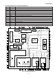

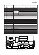

CD-PC1881V
– 46 –
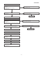
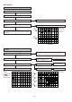
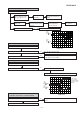
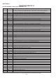
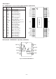
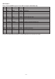
IC2 VHiLC78631E-1: Servo/Signal Control (LC78631E) (1/2)
Pin
No.
FunctionTerminal Name Input/Output
In this unit, the terminal with asterisk mark (*) is (open) terminal which is not connected to the outside.
Note: The same potential must be to the power terminals (VDD, VVDD, LVDD, RVDD, XVDD).
Unused input ports of general-purpose input/output ports (I/O) must be connected to 0V or set output port.
1* VPDO Output Variable pitch PLL charge pump output.
2 PD02 Output Double-speed and mode playback PLL charge pump output.
3 PDO1 Output Normal-speed mode playback PLL charge pump output.
4 AVSS — Analog system ground. Normally 0V.
5 FR — Built-in VCO frequency range setting resistor connection.
6 AVDD — Analog system power supply.
7 ISET — PDO1 and PDO2 output current setting resistor connection.
8 TAI Input Test input. A pull-down resistor is built in.
9 EFMO Output EFM signal output.
10 VSS — Digital system ground. Normally 0V.
11 EFMI Input EFM signal input.
12 TEST1 Input Test input. A pull-down resistor is built in.
13,14 CLV+, CLV- Output Spindle servo control output. CLV+ outputs a high level for acceleration, and CLV-outputs a high
level for deceleration.
15 V/P Output Rough servo/phase control automatic switching monitor output. A high-level output indicates
rough servo, and a low-level output indicates phase control.
16,17 TEST2, TEST3 Input Test input. A pull-down resistor in built in.
18* P4 Input/Output I/O port.
19 HFL Input Track detection signal input. This is a Schmitt input.
20 TES Input Tracking error signal input. This is a Schmitt input.
21* PCK Output EFM data playback bit clock monitor. Outputs 4.3218 MHz when the phasw is locked.
22* FSEQ Output Synchronization signal detection output. Output a high level when the synchronization signal
detected from EFM signal matches the internally generated synchronization signal.
23 TOFF Output Tracking off output.
24 TGL Output Tracking gain switching output. Increase the gain when this pin outputs a low level.
25* THLD Output Tracking hold output.
26 TEST4 Input Test input. A pull-down resistor is built in.
27 VDD — Digital system power supply.
28,29 JP+, JP- Output Track jump output. JP+ outputs a high level both for acceleration during outward direction jumps
and for deceleration during inward direction jumps. JP- outputs a high level both for acceleration
during inward direction jumps and for deceleration during outward direction jumps.
30*,31*
SLD+, SLD- Output Slide output. This pin can be set to 1 of 4 levels by commands sent from the system control
microprocessor.
32 EMPH_B Output De-emphasis monitor. A high level indicates that disc requlring de-emphasis is being played.
33* P5 Input/Output I/O port.
34* LRCKO Output LR clock output.
35* DFLRO Output Digital filter outputs
LR data output. The digital filters can be turned off with the DFOFF command.
36* DACKO Output Bit clock output.
37* CONT1 Output Output port.
38 P0/DFCK Input/Output I/O port or digital filter bit clock input.
39 P1/DFIN Input/Output I/O port or digital filter data input.
40 P2 Input/Output I/O port. Used as the de-emphasis filter on/off switching pin in anti shock mode.
41 P3/DFLR Input/Output Port output or digital fllter LR clock input.
42 LRSY Output LR clock output.
43 CK2 Output Bit clock output. The polarity can be inverted with the CK2CON command.
44 ROMXA Output ROMXA pins Interpolated data output. Data that has been interporated can be output by
issuing the ROMXA command.
45 C2F Output C2 flag output.
46 MUTEL Output Left channel mute output.
47 LVDD — Left channel power supply.
48 LCHP Output Left channel P output.
49 LCHN Output Left channel N output.
50 LVSS — Left channel ground. Normally 0V.
One-bit D/A
converter pins