CODE : 00ZARM350UA1E LASER PRINTER AR-M350U/M450U MODEL AR-M350N/M450N OPTIONS AR-P14 [1] INTRODUCTION The AR-M350U/M450U and AR-M350N/M450N are minor change models based on the AR-M350/M450. This service manual only provides information on these minor changes. In addition to this service manual, the documents listed below are required to properly maintain these machines.
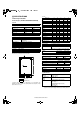
!"# "$ [3] CONFIGURATION 1.System Configurations Exit tray (AR-TE3 or AR-DU4 Standard) B/W scanner module/DSPF(AR-EF1) Duplex module/bypass tray(AR-DU4) Finisher (AR-FN6) Upper exit tray extension (AR-TE4) Duplex module (AR-DU3) Mail-bin stacker (AR-MS1) Saddle stitch finisher (AR-FN7) Stand/3 x 500 sheet paper drawer (AR-D14) Power supply unit (AR-DC1) Stand/MPD & 2000 sheet paper drawer (AR-D13) 2.
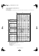
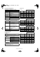
% !"# "$ 3. List of combination of peripheral devices A.AR-M350U/M450U As shown in the table below, some other peripheral devices ( B ) may be needed for installation of a peripheral device ( A ) and some peripheral devices cannot be installed together.
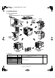
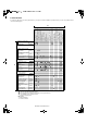
!"# "$ B.AR-M350N/M450N As shown in the table below, some other peripheral devices ( B ) may be needed for installation of a peripheral device ( A ) and some peripheral devices cannot be installed together.
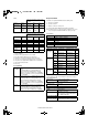
!"# $ [4] SPECIFICATIONS (in mm) 1. Basic Specification A B C D E A3 297 420 4 289 4 A. Base Engine (AR-M350U/M350N/M450U/M450N) B4 257 364 4 242 4 A4 210 297 4 202 4 B5 182 257 4 168 4 A5 148 210 4 140 4 Japanese postcard 100 148 4 92 4 Ledger 279 432 4 271 4 4 Paper size (1) Form AR-M350U/M350N/M450U/M450N Console type (2) Engine speed Paper size AR-M350U/N AR-M450U/N A4, 8.
% !"# $ B. Document Feeding Equipment (4) Print Function (1) One-drawer tray (included in the base engine) a. General Paper feed method Sizes to be fed Paper capacity Media available for paper feeding Paper type Paper size switching Dehumidification heater Balance detection Default size setting Mounting/demounting of the tray One-drawer tray A4, B5, 8.
!" # $ B. Expanded RAM e. Font When an optional PS3 expansion kit is installed Installation of an expanded RAM will avoid the following status.
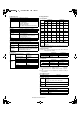
!"# $ (5) Image Process Half tone reproduction Exposure adjustment Quality selection Resolution* D. Copy function Equivalent to 256 levels Light / Auto / Dark Half-tone ON/OFF Normal ( 200x200dpi ) Fine ( 300x300dpi ) Super fine ( 400x400dpi ) Ultra fine ( 600x600dpi ) Varies with the file type/transmission method (1) Copy Speed AR-M350U/N AR-M450U/N Actual Reduction Enlargement Actual Reduction Enlargement A4, 8.5"x11" 35 35 35 45 45 45 A4R, 8.
' !"# $ (7) Copy Function Function APS AMS Paper type select Special function Standard Function Standard Function Standard Function (By type setting) Auto tray switching Standard Function Rotation copy Standard Function Electronic sort Standard Function Rotation sort Not provided Reserved copy Standard Function Prior tray setting Not provided Recall/register of program Standard Function Proof copy Not provided Preheat function Standard Function (To be set up by k
" #$%&'( [5] CONSUMABLE PARTS 1.Supply system table Note: The consumable parts are the same as those of the AR-M350/M450 and the AR-P350/P450. A.
"# $% & '( 2.Production number identification A. Drum cartridge C. Developer The lot number, printed on the front side flange, is composed of 10 digits, each digit showing the following content: The lot number is composed of 8 digit, and each digit indicates as following. The lot number shall be printed on the bag. 1 2 3 4 5 6 7 8 9 10 1 1 2 3 4 5/6 7 8/9 10 Number For this model, this digit is 2. Alphabet Indicates the model conformity code.
" #$%& ' [6] UNPACKING AND INSTALLATION 1. Installing procedure flowchart There are many combinations between this machine and option units. For installing option units, observe the following procedures for efficiency. To install the devices efficiently, follow the procedure below. Some peripheral devices may have been installed as standard devices depending on the main unit model. Part of descriptions and illustrations may be different.
( " #$%& ' 2. AR-P14 installing procedure * * * This installation procedure is provided for use with the AR-M350U/ M450U series. To connect this machine to a network, a Print Server Card (NIC) ARNC5J must be installed to the multi-function controller board in advance. <3>Remove the control PWB unit. Remove the five screws that fix the control PWB unit to the main unit of the printer.
) " #$%& ' <6>Connect the cables to the control PWB. Connect all the cables that have been removed in <2> to the original positions of the control PWB unit. 3) Prepare to enable the printer expansion function. To enable the printer expansion function, use the keys on the operation panel to enter the product key. For entry of the product key, see the key operator's guide of the operation manual for the main unit.
! [7] MAINTENANCE 1. Self print of set values Use SIM 22-6 to print the set values (machine settings) and jam history. These values must be printed before execution of maintenance or disassembly procedures. 2. Maintenance System Table The maintenance system table is the same as that of the AR-M350/M450. A. Scanner / DSPF Maintenance cycle : 50K Check (Clean, replace, or adjust as necessary.
" ! B. Engine section * For disassembly procedures, refer to the AR-P350/P450 Service Manual. Maintenance cycle : 50K Check (Clean, replace, or adjust as necessary.
# ! C. Peripheral devices Maintenance cycle : 50K Check (Clean, replace, or adjust as necessary.
!" #$ [8] SIMULATION Item For the simulation, the following items have been changed. MACHINE 22-10 Purpose Function (Content) Display Content AR-P350/350LP AR-P450/450LP Adjustment, setup, operation data output, check (display) Used to check the system configuration (option, internal hardware).
!"#!$ [9] CIRCUIT DIAGRAM 1. MFP Control PWB(for AR-M350U/M450U) A.
% !"#!$ CPU Block Regulator IC2 1.5V(Core) 5V Engine I/F CN13 3.3V(I/O) Clock buffer IC9 OSC X3 66.666Mhz TDI, TMS, TDO ,TCK, TRST* CPU TMPR4955AF 200Mhz IC20 160pin-QFP JTAG CN10 5V COLDRST CPURST 3_EXTRQST PONRST NMI, INT0* Reset IC PST598DN IC47 3.
& !"#!$ ROM Block ( Flash & Mask ) 3.
' !"#!$ SDRAM Block ( Standard & Option ) OSC X3 66.
( !"#!$ PCI Block ( ICU & Option ) PCI-Bus System Controller IC19 456pin-BGA SDRAM IC22, IC27 24MB Scanner I/F CN8 LVDS IC18 ICU ASIC IC25 304pin-QFP PM2500 IC13 160pin-QFP OSC X1 66.66Mhz Selector IC14 OSC X5 68.5Mhz Engine I/F CN13 OSC X2 40.57Mhz Buffer IC8 OSC X4 31.55.Mhz JCI-NIC (100Base-T) CN2 no support for STD control PWB J CN12 AR-M350U CIRCUIT DIAGRAM 9-5 HDD-PWB (2.
) !"#!$ I/O Block ( EEPROM & Misc I/O ) LVX161284 IC15 IEEE1284 I/F System Controller IC19 456pin-BGA CN1 DS14C238 IC42 RIC I/F (RS232C) IOA[15:1] CN14 16373 IC34 I/O G/A CN13 Scanner I/F TD62503F IC38 245 IC31 IC32 240pin-QFP Engine I/F TD62503F IC41 IOD[7:0] CN8 LCD Controller IC53 JP4,5 OSC X7 14.7456Mhz Xtal 32.
* !"#!$ AR-M350U CIRCUIT DIAGRAM 9-7
+ !"#!$ B. Circuit Diagram 5 4 3 [DRAGON-D10][CPU TX4955] + C125 D 3.3V 10uF/16V R127 R126 10 10 C130 C129 0.1uF 1000pF BR26 SYSADC2 SYSADC3 SYSADC0 SYSADC1 8 7 6 5 1 2 3 4 R136 R137 10 10 SYSADC[3:0] SYSADC3 SYSADC0 160 159 158 157 156 155 154 153 152 151 150 149 148 147 146 145 144 143 142 141 140 139 138 137 136 135 134 133 132 131 130 129 128 3.3V C R123 R122 10K 4.
D15 EL0 3 2 1 0 O VCCIO MASTERCLOCK VSS VCCPLL PLLCAP VSSPLL VCCIO VSS VCCIO PCST4 PCST5 PCST6 PCST7 PCST8 SYSAD3 VSS VCCINT SYSAD2 SYSAD1 VSS VCCIO SYSAD0 SYSADC1/(GND) VSS VCCINT SYSADC0/(GND) VSS VCCIO SYSADC3/(GND) VSS VCCINT SYSADC2/(GND) SYSAD31 VSS VCCIO SYSAD30 VSS VCCINT SYSAD29 SYSAD28 160 159 158 157 156 155 154 153 152 151 150 149 148 147 146 145 144 143 142 141 140 139 138 137 136 135 134 133 132 131 130 129 128 127 126 125 124 123 122 121 D6 O D7 D8 NT 3 D12 O D13 D14 NT O D4 D5 NT IC
!"#!$ A B C [Print Controller (for AR-M350U / M450U) (1/3)] 5 4 SYSCMD[8:0] IC19A CKE SYSCMD8 SYSCMD7 SYSCMD6 SYSCMD5 SYSCMD4 SYSCMD3 SYSCMD2 SYSCMD1 SYSCMD0 AA1 AA2 AA3 Y4 AB1 AB2 Y5 AA5 AA4 Y3 W4 Y2 V5 W3 Y1 W2 V4 W1 V3 V2 V1 U4 U3 T5 U2 U1 T4 T3 T2 R5 R4 T1 R3 R2 P4 R1 P3 P2 P1 N1 N2 N3 M1 N4 M2 M3 L1 M4 L2 L3 L4 K1 K2 L5 K3 K4 J1 J2 J3 H1 J4 H2 G1 J5 H3 H4 G2 G3 F1 F2 G4 F3 E1 6 SYSAD[54:33] 4 4,6 SYSAD54 SYSAD53 SYSAD52 SYSAD51 SYSAD50 SYSA
C !"#!$ D E BR18 8 7 6 5 1 2 3 4 R64 R65 BR7 8 7 6 5 10 10 1 2 3 4 MAA12 1 2 3 4 MAA11 MAA10 MAA9 MAA8 1 2 3 4 MAA7 MAA6 MAA5 MAA4 1 2 3 4 MAA3 MAA2 MAA1 MAA0 CKEA MRASA MCASA MWE 5 5 5 5 BSEL1A BSEL0A 5 5 MCS2A MCS1A MCS0 5 5 5 MAA[12:0] 5 5 BR19 CKE MRAS_ MCAS_ MWE_ BSEL1 BSEL0 MCS_4 MCS_3 MCS_2 MCS_1 MCS_0 MAD12 MAD11 MAD10 MAD9 MAD8 MAD7 MAD6 MAD5 MAD4 MAD3 MAD2 MAD1 MAD0 MD63 MD62 MD61 MD60 MD59 MD58 MD57 MD56 MD55 MD54 MD53 MD
% !"#!$ A B C [Print Controller (for AR-M350U / M450U) (2/3)] 3.3V IC19B C54 C106 22uF/16V 22uF/16V + C100 0.1uF C64 + 0.1uF C57 2.5V E14 N5 P22 AB13 4 C96 0.1uF C53 0.1uF C88 0.1uF C128 22uF/16V + 22uF/16V + 0.
& !"#!$ C D E IC19D L26 M24 M25 N23 BR42 4 3 2 1 5 6 7 8 L24 L25 M22 M23 BR46 1 2 3 4 8 7 6 5 L22 K25 K26 L23 B20 C20 B21 3.3V BOOTCS_ DREQ3_ DREQ2_ DREQ1_ DREQ0_ CODECS3_ CODECS2_ CODECS1_ CODECS0_ DACK3_ DACK2_ DACK1_ DACK0_ FONTCS7_ FONTCS6_ FONTCS5_ FONTCS4_ FONTCS3_ FONTCS2_ FONTCS1_ FONTCS0_ DMA_TC3_ DMA_TC2_ DMA_TC1_ DMA_TC0_ SCLK ADV_ BUFOE_ BUFDIR TXD1 RXD1 BR45 4 3 2 1 3.
' !"#!$ A B C [Print Controller (for AR-M350U / M450U) (3/3)] IC19C 5 1 A_SYSCMD[8:0] SYSCMD[8:0] A_SYSCMD8 R96 10 SYSCMD8 8 7 6 5 SYSCMD3 SYSCMD2 SYSCMD1 SYSCMD0 8 7 6 5 SYSCMD7 SYSCMD6 SYSCMD5 SYSCMD4 2 PCICLKI PCICLKO BR44 A_SYSCMD3 A_SYSCMD2 A_SYSCMD1 A_SYSCMD0 1 2 3 4 A_SYSCMD7 A_SYSCMD6 A_SYSCMD5 A_SYSCMD4 1 2 3 4 PCIMODE PCI_CBE3 PCI_CBE2 PCI_CBE1 PCI_CBE0 BR43 1 A_SYSAD[31:0] SYSAD[31:0] 2,6 PCIAD31 PCIAD30 PCIAD29 PCIAD28 PC
( !"#!$ C D E PCLK_D 21 PCLK_DR 21 IC19C SYSCMD[8:0] 2 5 PCICLKI PCICLKO PCIMODE PCI_CBE3 PCI_CBE2 PCI_CBE1 PCI_CBE0 E16 C17 B17 C8 A7 B8 D9 1 BR68 2 3 4 PCBE03 PCBE02 PCBE01 PCBE00 8 7 6 5 PCBE0[3:0] 17,18 PCIAD[31:0] SYSAD[31:0] 2,6 PCIAD31 PCIAD30 PCIAD29 PCIAD28 PCIAD27 PCIAD26 PCIAD25 PCIAD24 PCIAD23 PCIAD22 PCIAD21 PCIAD20 PCIAD19 PCIAD18 PCIAD17 PCIAD16 PCIAD15 PCIAD14 PCIAD13 PCIAD12 PCIAD11 PCIAD10 PCIAD9 PCIAD8 PCIAD7 PCIAD6 PCI
) !"#!$ A B C [SDRAM] 5 2 MWE 2 2 2 MCS0 MRASA MCASA 2 2 2 2 3_MD[63:0] 2 SDQMA[7:0] 2 MAA[12:0] 2 2 BSEL0A BSEL1A IC4 4 MAA0 MAA1 MAA2 MAA3 MAA4 MAA5 MAA6 MAA7 MAA8 MAA9 MAA10 MAA11 MAA12 23 24 25 26 29 30 31 32 33 34 22 35 36 3.3V 40 C11 0.
* !"#!$ C D E 5 2 MAA[12:0] 2 SDQMA[7:0] 2 3_MD[63:0] 3.3V 3.