
Datasheet
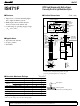

IS471F
*5 Defined as E
ep
that causes the output to go“ Low to High”
(
or“ High to Low”
)
.
■ Electro-optical Characteristics
(
V
CC
= 5V, Ta= 25˚C
)
Parameter Symbol Conditions
Operating supply voltage V
CC
Supply current I
CC
V
O
, GL
out
terminals shall be opened.
Output
V
OL
I
OL
= 16mA, E
VP VD
=0
*3
V
OH
E
VD
=E
VP
=0
*3
I
OS
E
VP
=E
VD
=0
*3
I
GL
V
GL
= 1.2V
t
p
t
W
E
ePLH
E
eD
=0
*3
Light emitting
E
ePHL
Hysteresis E
ePLH
/E
ePHL
Response
time
t
PHL
t
PLH
*7
External disturbing light illuminance
E
VDX
*3 E
eP
represents illuminance of signal light in sync with the low level timing of output at GL
out
terminal.
Fig.1
Fig.2 Fig.3
*4 Pulse cycle
(
t
P
)
, pulse width
(
t
W
)
are defined as shown in Fig. 2.
E
eD
represents illuminance of DC light. For detail, see Fig. 1.
E
VP
represents illuminance of signal light in sync with the low level timing of output at GL
out
terminal.
E
VD
represents illuminance of DC light. Note that the light source is CIE standard light source A.
shown in Fig. 3
(
Note
)
Fig. 1 shows the output waveform at GL
out
Fig. 3.
0
Time
Output waveform
E
e
E
eD
E
eP
at GL
out
terminal
5V
0V
IS471F
GND
280Ω
5V
0.33 µF
t
W
t
P
V
CC
V
O
GL
out
Light source: Infrared light emitting diode
(
λ p= 940nm
)
GL
output
MIN. TYP. MAX. Unit
4.5 - 16 V
-
-
-
-
3.5 7.0 mA
- 0.15 0.35 V
4.97 - - V
0.25 0.5 1.0 mA
40 55 70 mA
70 130 220 µ s
4.4 8 13.7 µ s
- 0.4 2.66
- 0.7 2.8
0.45 0.65 0.95 -
- 400 670 µ s
- 400 670 µ s
2000 7500 -
Low level output voltage
High level output voltage
Output short circuit current
Low level output current
diode
(
λ p= 940nm
)
*6
µ W/mm
2
µ W/mm
2
terminal with IS471F connected as shown in
The waveform shown in Fig. 2 is the output voltage waveform at GL
out
terminal with IS471F connected as
*5
“Low→High ” threshold irradiance
*5
“High→Low ” threshold irradiance
Eep= 7.5 µ W/mm
2
,
*3
λ p= 940nm
*4
Pulse cycle
*4
Pulse width
*6
*6
“ High
→Low”
propagation delay time
“ Low→High”
propagation dealy time
1
2
4
3
= 500lx, E
lx