MD-R2 SERVICE MANUAL No. S1805MDR2//// MD-R2 • In the interests of user-safety the set should be restored to its original condition and only parts identical to those specified should be used. CONTENTS Page IMPORTANT SERVICE NOTES ............................................................................................................................................ 2 SPECIFICATIONS .........................................................................................................................
MD-R2 FOR A COMPLETE DESCRIPTION OF THE OPERATION OF THIS UNIT, PLEASE REFER TO THE OPERATION MANUAL. IMPORTANT SERVICE NOTES BEFORE RETURNING THE AUDIO PRODUCT (Fire & Shock Hazard) Before returning the audio product to the user, perform the following safety checks. 1. Inspect all lead dress to make certain that leads are not pinched or that hardware is not lodged between the chassis and other metal parts in the audio product. 2.
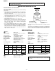
MD-R2 NAME OF PARTS Front panel 1 11 12 13 2 3 4 5 TOC DISC TRACK DATE MONO LP PRGM TOTAL REMAIN RANDOM 14 1516 17 18 6 12 TIMER REC 19 7 4 0dB 8 OVER 9 10 AM 1 2 3 4 5 6 7 PM 8 9 10 11 12 13 14 CLOCK 15 16 17 18 19 20 20 21 22 23 24 25 26 27 28 29 30 31 32 33 34 36 37 20. Clock Indicator 21. Eject Button: 22. Remote Sensor 23. Cue/Review Button: 24. Display/Character Button 25. Name/TOC Edit Button 26. Record Level Control 27. Headphone Level Control 28. Headphone Jack 29.
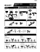
–4– 7 AM CLOCK TIMER DELETE/CLEAR AM CLOCK Time setting mode DATE Each time the button is pressed, the display will change. Date setting mode DATE CLOCK ENTER 5 6 7 4 3 2 1 The unit will enter the time setting mode. Set the “day” repeating steps 4 and 5. Set the “month” repeating steps 4 and 5. Press the ENTER button to set the “year”. When you turn the jog dial and let go, the year will change up or down by one.
11 10 9 8 (Continued) DATE DATE DATE DATE PM CLOCK PM CLOCK PM CLOCK PM CLOCK ENTER TIMER DELETE/CLEAR When you turn the jog dial and let go, the hour will change up or down by one. When you turn and hold it, the hour will change continuously. The clock uses the 12-hour system. Pay attention to the AM or PM indicator in the display. AM 0:00 → midnight, PM 0:00 → noon Set the “hour” using the jog dial. –5– Once you have set the date and time, “TIME ADJUST” will not be displayed in step 2.
SYMPTOM SYMPTOM –6– Replace the batteries. Operate it within a range of 8" (0.2 m) to 20' (6 m) and within an angle of 15 o to either side of center. Load a disc. Connect the AC power cord. The batteries inside the remote control are dead. The remote control is operated from an incorrect distance or angle. No disc has been loaded. Is the AC power cord plugged in? The power cannot be turned on from the remote control. Insert properly.
MD-R2 Quick-Guide Guía rápida MINIDISC DECK MD-R2 Turning the power on and off Conexión y desconexión de la alimentación Connection Conexión • Stereo, DAT, MD recorder, etc. • Equipment with a • MD/CD player with an optical input/output jack coaxial jack • Equipo con toma coaxial Remote control Control remoto etc. • Estéreo, DAT, grabadora de • Reproductor MD, etc. con toma de entrada/salida óptica de MD/CD etc.
MD-R2 DISASSEMBLY Caution on Disassembly Follow the below-mentioned notes when disassembling the unit and reassembling it, to keep it safe and ensure excellent performance: 1. Take the minidisc out of the unit. 2. When disassembling the machine, be sure to withdraw the power plug from the socket in advance. 3. When disassemble the parts, remove the nylon band or wire holder as necessary. To assemble after repair, be sure to arrange the wires as they were.
MD-R2 ( L2 ) x 1 Pickup Flexible PWB (*1) MD Mechanism MD Main PWB ( L1 ) x 4 ø1.7 x 3mm Pull (L2)x1 (*1) After disconnecting the optical pickup flex PWB from the connector wrap the front end of flex PWB in conductive aluminium foil so as to prevent electrostatic damage of optical pickup. ( L2 ) x 1 ( L2 ) x 3 Frame (M1)x4 ø1.7x8.
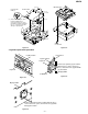
MD-R2 REMOVING AND REINSTALLING THE MAIN PARTS (A1)x1 ø1.7x5mm MD MECHANISM SECTION Perform steps 1 to 3 of the disassembly method to remove the MD mechanism. Magnetic Head How to remove the magnetic head (See Fig. 10-1) 1. Remove the screws (A1) x 1 pc. Caution: Take utmost care so that the magnetic head is not damaged when it is mounted. MD Mechanism Figure 10-1 How to remove the cartridge holder (See Fig. 10-2) Slider Lever 1.
MD-R2 How to remove the sled motor/loading motor (See Fig. 11-1) 1. Remove the screws (D1) x 1 pcs., and remove the sled motor/loading motor. (D1)x2 ø1.7x2mm (D1)x2 ø1.7x2mm Caution: Be careful so that the gear is not damaged. (The damaged gear emits noise during searching.) Loading Motor Sled Motor Figure 11-1 How to remove the spindle motor (See Fig. 11-2) 1. Remove the screws (E1) x 3 pcs., and remove the spidle motor. Caution: Be careful so that the turntable is not damaged. Turntable (E1)x3 ø1.
MD-R2 ADJUSTMENT TEST MODE 1) Mode there are 5 kinds TEST MODE as below. MODE PUSH KEY A) MD TEST MODE ENTER PLAY B) AUDIO TEST MODE CUE REVIEW C) KEY TEST MODE CUE ENTER D) RECORDING TEST MODE ENTER REC E) MD TEST2 MODE (DATA MONITOR MODE) ENTER STOP 2) How to start and quit TEST MODE. AC Supply On or push RESET KEY after push two keys. In all TEST MODE. Power Off (POWER KEY) is quit TEST MODE. 3) TEST MODE description. A) MD TEST MODE (ENTER+PLAY) Disp. Will be "AUT YOBI".
MD-R2 KEY TEST KEY NAME TIMER KEY NAME ILLUMINATE SEGMENT 10 ROW DOT ILLUMINATE SEGMENT INPUT SELECT TOC DISPLAY 11 ROW DOT EJECT 7 ROW DOT REVIEW ALL PLAY 4 ROW DOT CUE PM STOP 5 ROW DOT ENTER 8 ROW DOT REC 6 ROW DOT JOG. UP 17 (M.C.) NAME 9 ROW DOT JOG. DOWN 18 (M.C.) TIME AM PROGRAM PRGM D) Recording test mode (ENTER+REC) This mode is auto recording repeat mode. After disc full. Erase all and rec start again. MD SECTION 1.
MD-R2 • Test Mode 1. AUTO pre-adjustment mode • Automatic pre-adjustment is performed. (After adjustment the grating adjustment mode is set.) • The adjustment value is output with the aid of system controller interface. 2. AUTO adjustment mode • Automatic adjustment is performed. • The adjustment value is output with the aid of system controller interface. • Continuous playback is performed. (Error rate indication, jump test) 3.
MD-R2 2. AUTO adjustment mode Step No. • Setting Method Remarks Display Step 1 Testmode STOP state Step 2 Press the ENTER button two times. [tsm Step 3 Press once the MD PLAY button. The slide moves to the innermost periphery, and automatic adjustment is started. • In case of high reflection disc changes as follows. PEG→HAG •In case of low reflection disc changes as follows. PEG→LAG→GCG→GEG→LAG End of adjustment If adjustment is OK, Step 4. If adjustment is NG, Step 7.
MD-R2 3. RESULT mode (final adjustment) Step No. Setting Method Remarks Display Step 1 Testmode STOP state [tsm Step 2 Press the ENTER button four times. Step 3 Press once the MD PLAY button. Indication of set value [HAG:__ _ Step 4 Press once the ENTER button. Indication of set value [HBG:__ _ ] Step 5 Press once the ENTER button. Indication of set value [LAG:__ _ ] Step 6 Press once the ENTER button. Indication of set value [LBG:__ _ ] Step 7 Press once the ENTER button.
MD-R2 • If the jog key upward/downward is pressed during setting indication, the setting increases/decreases, and the new setting is stored in RAM. • If the REC button is pressed, the setting returns step by step excepting the following case.
MD-R2 Setting Method Step No. Remarks Display Step 9 Press once the ENTER button. Comparison level setting in case of FOK generation (when focus is "ON") [FOKLEV f_ Step 10 Press once the ENTER button. LPF coefficient setting (normal) in case of FOK generation [FOKLPFn_ Step 11 Press once the ENTER button. LPF coefficient setting in case of FOK generation (when focus is "ON") [FOKLPFf_ Step 12 Press once the ENTER button.
MD-R2 Setting Method Step No. Remarks Display Step 18 Press once the ENTER button. TCRS comparison level 1 for high reflection [TCRSCIP_ Step 19 Press once the ENTER button. Comparison level in case of COUT generation (playback) [COTLVp__ ] ] Step 20 Press once the ENTER button. Comparison level in case of COUT generation (pecord) [COTLVr__ ] Step 21 Press once the ENTER button.
MD-R2 e) TEMP setting Setting Method Step No. Remarks Step 1 Testmode STOP state Step 2 Press the ENTER button seven times. Step 3 Press once the MD PLAY button. Focus setting menu [tsm EEPROM setting menu ] [__Focus___] Press the ENTER button four times. Step 5 Press once the MD PLAY button. TEMP reference value setting TEMP setting menu Setting Method e [E E P R O M _ S E T] Step 4 Step No.
MD-R2 8. TEST-PLAY mode Setting Method Step No. Remarks Display Step 1 Testmode STOP state [tsm Step 2 Press the DELETE/CLEAR button. TEST-PLAY menu [TEST_PLAY_] Step 3 Press once the DISPLAY button. ADRES setting (Target address initial value is indicated) Press once the MD PLAY button. During search the search output pin 11 is set to "H", and it is returned to "L" when continuous playback is started.
MD-R2 10. INNER mode Setting Method Step No. Remarks Display Step 1 Testmode STOP state [tsm Step 2 Press the NAME/TOC EDIT button. INNER menu [__INNER__] e Step 3 Press once the MD PLAY button. INNER switch position measurement (SUBQ address and C1 error are also indicated.) [s Step 4 Press once the MD STOP button. INNER menu [__INNER__] c ] ] : Adress • • Press the MD STOP button while the INNER menu is displayed, to shift to the TEST mode STOP state. 11. EJECT mode Step No.
MD-R2 Mechanism Adjustment 1.
MD-R2 EXPLANATION OF ERROR DISPLAY Error display Corrective action Errors Can't REC • Defect occurred successively 10 times during REC-PLAY. • Check that the disc is free from flaw, dust • As a result of occurrence of defect during REC-PLAY the and fingerprint. recordable cluster became zero. Check whether there is any black spot. • Adress is unreadable. REC state connot be set for 20 seconds Check for disc disalignment and run-out. although retry is repeated.
MD-R2 Error display Corrective action Errors BLANK MD • UTOC was read but total TNO and the number of characters of • Perform recording to check that the disc is recordable disc. NAME was 0? DEFECT • Focusing error was caused by shock during REC-PLAY. • Check that the disc is free from flaw, dust, fingerprint and black spot. Check for disc disalignment and run-out. TOC W ERROR • Although UTOC can be read but UTOC cannot be rewritten. • Check that the record head contact is normal.
MD-R2 E2-PROM Data List Slide setting Focus setting Item indication Item indication Initial Setting Initial Setting FG 97 H SLG 35 H FF1 9E H SL2 27 H H SLDLIM 65 H FF2 E0 FZHLEV ED H SLDLEV 16 H FOKLEVn 08 H SLKLVk 55 H FOKLEVf 08 H SLKLVt 3A H FOKLPFn 00 H SLKLVm 55 H FOKLPFf 88 H WAITf 90 H Control setting Item indication Spin setting Item indication SPG Initial Setting 20 SPG—in SPG—mid B8 76 H H H SPG—out 50 H SP1 10 H SP2 87 H SP3 E3
MD-R2 E2-PROM Setting Mode Chart tms e Test mode STOP state ENTER X7 E E P R O M _ S E T EEPROM setting menu _ _ EJECT _ _ _ MD PLAY EJECT state _ _ Focus_ _ _ MD PLAY ENTER ENTER X2 _Spindle__ MD PLAY FG______ ENTER REC ENTER REC ENTER WAITf___ REC REC ENTER ENTER ENTER ENTER ENTER ENTER REC ENTER ENTER REC ENTER ENTER REC ENTER REC REC REC REC ENTER REC ADJTTM__ ENTER REC HDEQAD__ ENTER REC LDEQAD__ REC ENTER REC GDEQAD__ ENTER ENTER REC REC REC REC RE
Figure 28 BLOCK DIAGRAM (1/2) – 28 – M M903 LOADING MOTOR HEAD UP/DOWN M M902 SLED MOTOR M DIRECT SWITCH SW1952 LEAD INSWITCH SW1953 PLAYSWITCH SW1954 RECSWITCH SW1955 LOADING SWITCH SW1956 WRITE PRO LIGHT RECEIVING SECTION RF LIGHT RECEIVING SECTION ERROR SIGNAL MD Q1251~Q1254 D4.3V IC1601 M56758FP 5-CH MOTOR DRIVER MONITOR DIODE LASER DIODE IC1101 IR3R55 RF SIGNAL PROCESSOR D3.2V D6.5/4.75 ~ 5.25V D4.
– 29 – UN970 REMOTE SENSOR KEY IN BLOCK JOG SWITCH SW901 RX302 DIGITAL IN (OPTICAL JACK) TX302 DIGITAL OUT (OPTICAL JACK) J301 1 DIGITAL -IN (COAXIAL JACK) INVERTER IC301 74HCU04 6 KEY JOG +7V 10 13 8 45 ~ 90 92 ~ 97 DIG SEG 21 ~ 42 60 ~ 89 FL901 2 IC302 NAND GATE 74HC10AP -7V 12 16 ~ 19 FL DISPLAY +B DIGIN VCC DIGITAL OUT MD UNIT DIGITAL IN 17 ~ 21 24 26 10 2 13 ~ 15 IC201 UDA1340 AD/DA CONVERTER IC901 IX0237AW SYSTEM MICROCOMPUTER 3 5 SYSCLK AD DATA LRCLK 1 7 BLCK DA DATA
MD-R2 DIGITAL RECORD SIGNAL DIGITAL PLAYBACK SIGNAL A ANALOG PLAYBACK SIGNAL ANALOG RECORD SIGNAL R607 1K (0.6V) R601 470 C601 47/10 C107 1/50 R103 1K R109 1K (1/2) C109 220P C105 220P +7V R113 1K L-CH R60 1K L-CH 7 6 – R115 100 C117 100/10 R111 1.5K R605 22K 8 R107 100K B C115 47/10 5 + R105 47K C60 220 C603 220P IC101 NJM4560D OPE AMP. R608 1K (0.8V) C113 47P R602 470 C602 47/10 C604 220P J101 ANALOG LINE IN2 L101 0.22µH R-CH C102 0.
MD-R2 C451 47/10 IC601 NJM4580D LINE AMP. R601 470 R609 1K R608 1K R602 470 C604 220P R613 100 C615 100/10 C611 47P (2/2) 7 R653 1K R614 100 C651 150P R651 100K C652 150P R652 100K IC651 NJM4560D OPE AMP. 5 + (1/2) C653 27P C655 10/16 R616 47K –7V R681 1K C454 470P R452 R458 330 10K C460 470P Q452 2SC2878 B C452 47/10 MUSE R620 10K Q602 2SC2878 B R-CH 4 R612 1.
MD-R2 A HEADPHONES PWB-B3 CNS903 B CNP473 P31 12 - C AUX_VR_L_OUT GND OPEN AUX_VR_R_OUT HP_AMP_GND HP_AMP_L_OUT HP_AMP_R_OUT RESET SW 10 NC 12 11 C981 0.001 VR901-2 5K(B) VR981-1 1K(C) VR981-2 1K(C) Headphone Volume J981 HEADPHONES R L VR901-1 5K(B) AUX Volume 1 2 3 4 5 6 7 8 9 3 2 1 CNS901 C983 0.1 C982 0.001 TO MAIN PWB AUX_AMP_R_IN AUX_AMP_L_GND AUX_AMP_L_IN AUX_AMP_R_GND 3 2 1 CNP904 L901 22µH D 21 20 R968 10K 19 18 R969 10K 17 16 DAC DATA DFS MD DSCK MD K-DATA 15 MD 7.
MD-R2 C914 0.001 C915 0.001 IC USEG31 USEG32 USEG33 USEG34 USEG35 USEG36 UDIG16 UDIG15 UDIG14 UDIG13 UDIG12 UDIG11 UDIG10 UDIG09 UDIG08 UDIG07 UDIG06 UDIG05 UDIG04 UDIG03 UDIG02 UDIG01 FILMNT1 FILMNT1 FILMNT1 FL901 FILMNT2 FILMNT2 FILMNT2 C916 0.001 C917 0.
MD-R2 1 SYRS SYRD SYWR SYD7 A AOUT BIN BOUT EIN EOUT LOGIC 21 22 23 24 LATCH 25 TP1134 R1152 22K TP1133 R1151 22K TP1132 R1150 22K 11 C1211 1 12 13 14 15 16 TP1220 FODRF FODRR TRDRF TRDRR SLDRF SLDRR SPDRF SPDRR R1653 100K R1651 R1657 R1655 R1661 R1659 R1665 17 100K 120K 120K 82K 82K 62K 18 19 20 21 22 23 24 25 R1663 62K SYRS X176KO FODRF FODRR TRDRF TRDRR SLDRF SLDRR SPDRF SPDRR 2 26 27 28 C1210 20 DVCC 19 DATA 18 26 10 WBO-I DATA 17 LATCH 16 TP1135 R1153 22K FOUT
MD-R2 6 R1211 220 18 19 20 21 22 23 24 25 R1663 62K TP1218 TP1217 XRST SYD7 SYD6 SYD5 SYD4 SYD3 SYD2 SYD1 SYD0 RSTX DGND VDD1 DINTX MCCK COUT SENSE FOK SFSY SBSY SBO X176KO FODRF FODRR TRDRF TRDRR SLDRF SLDRR SPDRF SPDRR SBCK TEMON TOTMON 48 49 50 26 27 28 TP1212 TP1213 23 22 66 65 64 C1203 1 63 62 R1202 1M R1201 150 XL1201 33.8688MHz C1204 12P(CH) C1205 12P (CH) 61 60 59 58 57 56 TP1273 55 53 TP1214 8 R1969 C1958 56 0.047 CLOCK GENERATOR C1954 15P (CH) R1963 1.
MD-R2 A P39 9 - H TO MAIN PWB CNP471 Q1820 R1456 Q1822 L1950 C1252 Q1253 Q1254 7 1 Q1403 Q1404 Q1451 Q1821 C1425 C1255 R1460 R1458 R1454 R1452 R1464 R1462 R1466 C1724 LR190 R1994 TO MAGNETIC HEAD P41 9 - H R1251 R1708 R1733 C1251 R1827 R1939 R1940 IC1251 C1927 C CN1252 2 1 D1251 1 Q1252 L1251 CN1902 24 C1254 B D1252 MD MAIN PWB - E (TOP VIEW) 1 Q1251 24 R1223 14 8 8 IC1906 3 4 R1963 7 50 26 45 40 30 35 1 25 55 60 C1211 R1202 5 80 75 85 90
MD-R2 P39 8 - A TO MAIN PWB CNP301 MD MAIN PWB - E (BOTTOM VIEW) TP1504 TP1516 TP1518 TP1502 R1805 Q1807 TP1901 Q1802 Q1803 TP1803 TP1506 R1424 R1422 R1404 R1401 R1472 C1402 TP1509 TP1510 TP1456 TP1713 TP1416 TP1457 TP1278 81 51 31 50 7 BK BLACK PK PINK C1653 TP1605 TP1616 TP1609 R1664 C1654 30 C1605 TP1610 C1655 25 R1650 8 C1602 R1658 TP1608 C1601 C1651 R1652 C1650 TP1220 15 C1657 22 TP1102 TP1611 R1660 20 2 1 C1661 CNP1604 C1652 R1654 R1281 C1116 TP1
MD-R2 A COAXIAL DIGITAL 2 IN J301 AC POWER OPTICA SUPPLY CORD (216) OUT TX302 C315 AC 120V, 60Hz D301 R301 1 2 3 C301 R304 R310 R308 7 IC301 C310 1 R312 R305 C312 C313 C305 C304 C311 L302 L301 1 8 CNP301 IC302 C D512 C522 R313 7 C303 14 D513 8 14 Q504 B C E T551 POWER TRANSFORMER 1 2 3 4 C525 C221 R510 R509 C513 D D505 T.
MD-R2 P37 8 - A TO MAIN PWB 2 IN CN1904 OPTICAL IN1 RX302 SW501 RESET C457 C119 Q451 C604 C212 C223 C519 C524 R403 R404 R401 R409 R407 R406 R408 C652 L202 C531 D651 C470 Q653 CNP471 CNP472 C675 1 8 R669 R105 C105 C107 24 CN1902 P40 5 - C TO DISPLAY PWB 7 B C E R552 R553 1 CNP902 3 2 1 C667 1 3 5 7 9 11 13 15 17 19 21 23 2 4 6 8 10 12 14 16 18 20 22 24 R554 C530 IC501 L201 24 22 20 18 16 14 12 10 8 6 4 2 23 21 19 17 15 13 11 9 7 5 3 1 R506 R505 1 4 C656 C220 24
MD-R2 DISPLAY PWB-B1 VR981 A 1 2 3 CNS901 1 C983 C982 C981 1 2 3 CNP904 HEADPHONE VOLUME 1 1 2 3 4 5 6 7 8 9 10 11 12 3 SW957 NAME SW958 TIMER J981 HEADPHONES B VR901 AUX VOLUME HEADPHONES PWB-B3 SW959 DISP 12 R956 P39 12 - D CNP473 TO MAIN PWB CNS903 R957 R955 R958 R959 R953 SW954 CUE R954 R926 R960 RA930 SW956 ENTER R905 C906 P39 8 - H SW901 JOG 1 CNP472 TO MAIN PWB RA926 R924 RA933 RA925 1 2 3 4 C907 5 6 RA931 RA919 R923 7 8 R920 9 RA928 10 Q901 11 12 SW962 RA916 RA91
MD-R2 MD SPINDLE M901 TO MD MAIN PWB CN1603 P36 1 - G RD 1 BK 2 MD SLED M902 TO MD MAIN PWB CN1602 P36 1 - E RD 1 BK 2 MD LOADING M903 TO MD MAIN PWB CN1604 P37 12 - F RD 1 BK 2 COLOR TABLE P37 12 - E TO MD MAIN PWB CN1601 SW1953 LEAD IN SW1955 RECORD SW1954 PLAY R1904 2 4 1 3 5 CN1901 CW1901 R1903 R1902 BR BROWN RD(R) RED OR ORANGE YL YELLOW GR GREEN BL BLUE VL VIOLET GY GRAY WH(W) WHITE BK BLACK PK PINK R1901 SW1956 LOADING SW1952 DIRECT MD MECHANISM SWITCH PWB-C
MD-R2 VOLTAGE (MD MAIN PWB) Q1801 PIN NO. E C B VOLTAGE 5V 5V 43V Q1802 PIN NO. E C B VOLTAGE 0V 0V 0.15V Q1803 PIN NO. E C B VOLTAGE 0V 0V 3.1V Q1807 PIN NO. E C B VOLTAGE 3.95V 3.2V 3.3V Q1820 PIN NO. E C B VOLTAGE 3.2V 3.18V 2.4V Q1821 PIN NO. E C B VOLTAGE 0V 0V 3.08V Q1822 PIN NO. E C B VOLTAGE 0V 0V 0.1V Q1451 PIN NO. E C B VOLTAGE 0V 3.18V 0.1V Q1401 PIN NO. E C B VOLTAGE 3.2V 3.2V 0V Q1402 PIN NO. E C B VOLTAGE 0V 0V 2.3V Q1403 PIN NO. E C B VOLTAGE 3.18V 0V 3.
MD-R2 NOTES ON SCHEMATIC DIAGRAM • Resistor: To differentiate the units of resistors, such symbol as K and M are used: the symbol K means 1000 ohm and the symbol M means 1000 kohm and the resistor without any symbol is ohm-type resistor. Besides, the one with “Fusible” is a fuse type. • Capacitor: To indicate the unit of capacitor, a symbol P is used: this symbol P means micro-micro-farad and the unit of the capacitor without such a symbol is microfarad.
MD-R2 WAVEFORMS OF MD CIRCUIT PLAY STATE Stopped NORM: 100M S/s CH1 500mV AC 10:1 CH1 2V DC 10:1 500ns/div 1 Offset TP1274 (EFMMON) CH1 CH2 CH3 CH4 T --0.000V 0.000V 0.000V 6 Record Len Main 500 Zoom 10 1 1997 / 08 / 04 13:35:24 T Filter SMOOTH OFF BW FULL 1 PIT PLAY Stopped NORM: 1M S/s 1997 / 08 / 04 09:30:15 T CH2 2V DC 10:1 CH3 200mV AC 10:1 CH4 5V DC 10:1 1ms/div Filter SMOOTH OFF BW FULL TP1274 1 TP1218 (TEMON) T Record Len Main 10K Zoom 100 2 Detay 0.
MD-R2 Stopped NORM: 1k S/s CH1 2V DC 10:1 9 CH2 2V DC 10:1 CH3 5V DC 10:1 CH4 5V DC 10:1 1997 / 08 / 04 11:23:12 T CH1 5V DC 10:1 1s/div CH2 5V DC 10:1 CH3 52V DC 10:1 2us/div Filter SMOOTH OFF BW FULL TP1216 1 6 PLAY Stopped NORM: 100M S/s 1997 / 08 / 04 14:19:52 T Offset 0.000V 0.000V 0.000V 0.000V CH1 CH2 CH3 CH4 TP1218 T Filter SMOOTH OFF BW FULL T Record Len Main 10K Zoom 100 2 Detay 18 DADATA 20 BCLK CH1 CH2 CH3 CH4 1 Record Len Main 2K Zoom 20 Detay 0.
MD-R2 TROUBLE SHOOTING When MD fails operate If the objective lens of optical pickup is contaminated, MD may fail to operate. At first, clean the objective lens to check playback operation. If MD fails persistently to operate, perform checks as follows. If dust or foreign substance is accumulated on the pickup lens, playback is disturbed and indication of TOC (content of tracks) may be disabled. Before adjusting check that the lens is clean. If the lens is contaminated, treat it as follows.
MD-R2 • Disc loading is not normal. Yes Is disc loaded when it is inserted? No Check CNP1601 and SW1956. Is the pin 4 of CNP1601 set to L state? No Yes Is change observed on the pin 23 or 24 of IC1601? Check IC1401. No No Yes Is change observed on the pin 30 or 31 of IC1601? Check CNP1604 and IC1601. No Yes Check CNP1604 and CN1604 Yes Is ejection performed when the MD taking-out button is pressed? No Yes Disc retracts soon after completion of disc ejection. Yes Check CNP1601 and SW1956.
MD-R2 • Normal playback When it has been confirmed that EEPROM value is normal in the TEST mode Is initialization performed normally when high reflection disc is played back? Does the playback time display advance? Yes No No Check IC1201 Does disc rotate normally? No Is lead-in switch turned on in the TEST mode when the pickup is on the innermost periphery (Is the pin 6 of OC1401 on L level?) No Yes Is an attempt to read repeatedly the TOC section of low reflection disc made? Check SW1953, mechanism
MD-R2 • Record and playback operation Insert the low reflection disc, and after verifying the audio output in the normal mode playback set the record/playback TEST mode Recording from start address cannot be performed. Yes Is RF waveform output to the pin 1 IC1201 or TP1274 when playback is performed after recording? Check whether the disc is record-prohibited.
MD-R2 • Disc motor fails to run Does waveform appear on the pins 24 and 25 of IC1201 in the TEST mode focus gain coarse adjustment step? No Check soldering joint and parts of pins 24 and 25 of IC1201, and peripheral circuit. No Check soldering joint of PWB of completed IC1601 and CNP1601 disc motor. No Check the soldering joint of pins 20 and 21 of IC1201, IC1601, IC1601, CNS1101. Yes Check the waveform on the pins 22 and 23 of IC1201, check the peripheral parts and soldering joint.
MD-R2 FUNCTION TABLE OF IC IC901 RH-iX0237AFZZ: System Control Microcomputer (IX0237AW) (1/2) Port Name Pin No.
MD-R2 IC901 RH-iX0237AFZZ: System Control Microcomputer (IX0237AW) (2/2) Pin No.
MD-R2 IC1101 VHiiR3R55//-1:RF Signal Control (IR3R55) Pin No. Function Terminal Name 1 RF1 RF signal input terminal 1 Input of RF signal output of pickup 2 RF2 RF signal input terminal 2 Input of RF signal output of pickup 3 RF3 RF signal input terminal 3 Input of RF signal output of pickup 4 RF4 RF signal input terminal 4 Input of RF signal output of pickup 5 REFI Reference voltage amp. input terminal 6 REFO Reference voltage amp.
MD-R2 IC1201 VHiLR376481-1:ENDEC/ATRAC (LR376481) (1/2) Pin No.
MD-R2 IC1201 VHiLR376481-1:ENDEC/ATRAC (LR376481) (2/2) Pin No. Function Terminal Name Input/Output 54 TESO1 Output 55 TESO3 In/Output PLLOSC. Microcomputer extension output port 3 in case of selection PLLLR. Microcomputer extension output port 2 in case of selection 56 TEST4 In/Output EXTCLK. Microcomputer extension output port 4 in case of selection 57* CDDATA In/Output High speed dubbing CD data input.
MD-R2 IC1401 RX-iX0232AWZZ:MD System Microcomputer (IX0232AW) (1/2) Pin No.
MD-R2 IC1401 RX-iX0232AWZZ:MD System Microcomputer (IX0232AW) (2/2) Pin No.
MD-R2 1 RF2 2 RF3 3 GOUT ATTR EFMAGI EFMAGC AGND AVCC EFMI EFMO RF2-1 ADAGI ADAGC 48 47 46 45 44 43 42 41 40 39 38 37 EFM AGC RESISTOR & SW RF1 POUT IC1101 VHiiR3R55//-1:RF Signal Control (IR3R55) 36 ADIPI 35 ADIPO DIFF 34 NC DIFF RF4 4 REFI 5 REFO 6 RFADD 7 TCGI 8 29 TCGO AIN 9 28 AOUT BIN 10 27 BOUT 33 ADLPFO ADIP AGC 32 22KO 31 22KI BIAS EIN 11 30 WBO HPF LPF 26 EOUT LOGIC 13 14 15 16 17 18 19 20 21 22 23 24 AVCC XSTBY XDISC X
MD-R2 PARTS GUIDE MODEL MD-R2 “HOW TO ORDER REPLACEMENT PARTS” To have your order filled promptly and correctly, please furnish the following information. 1. MODEL NUMBER 2. REF. No. 3. PART NO. 4. DESCRIPTION For U.S.A. only Contact your nearest SHARP Parts Distributor to order. For location of SHARP Parts Distributor, Please call Toll-Free; 1-800-BE-SHARP MARK: SPARE PARTS-DELIVERY SECTION Explanation of capacitors/resistors parts codes Capacitors Resistors VCC .......................
MD-R2 NO.
MD-R2 NO.
MD-R2 NO.
MD-R2 NO.
MD-R2 NO. PRICE RANK PART CODE PWB-C QPWBF0400AWZZ J PWB-D 92LPWB2604MDSS J DESCRIPTION NO.
MD-R2 608 8 48 611 16 35 A 45 611 12 10 5 B 11 18 611 609 608 CNS1252 611 29 39 51 C 30 40 B1 609 13 37 A1 607 B2 41 25 3 9 33 A 22 21 D A2 19 610 38 601 610 23 26 604 31 601 37 20 601 SW1956 17 601 38 607 605 607 42 607 E PWB-C 6 SW 1952 SW1955 CFW1901 603x2 SW1953 SW1954 1 15 50 32 CNW301 14 7 24 F 603x2 PWB-D 602 612x4 34 602 4 A1 B2 A G A2 B1 2 46 49 613 47 613 M902 M903 M901 H 606x3 1 2 3 4 Figure 6 MD MECHANISM EXP
MD-R2 606x3 225 A 606 606x5 B 602x5 215 604x3 609x4 611 PWB-B2 606 C 201 201-1 220 602 x10 214 210 FL901 201-2 PWB-B1 D MD Unit 212 209 211 601 208 207 E 603 203 Nut with SW901 Silicon Grease 213 603 607x2 PWB-B3 608x2 609 206 Washer with 204 SW901 605x4 228 612 205x2 PWB-A F 227x2 610 226x4 217 216 G 218 219 222x2 221x2 229 609x2 H 224 610x3 609x2 610 1 2 3 4 Figure 7 CABINET EXPLODED VIEW 7 –– –– 66 5 6
MD-R2 PACKING OF THE SET Polyethylene Bag, Accessories SSAKH0025AWZZ Remote Control Operation Manual Quick Guide Packing Add.
MD-R2 COPYRIGHT © 1998 BY SHARP COPORATION ALL RIGHTS RESERVED. No part of this publication may be reproduced, stored in a retrieval system, or transmitted in any from or by any means, electronic, mechanical, photocopying, recording, or otherwise, without prior written permission of the publisher.