MD-X5H/CP-X5H SERVICE MANUAL No. S0781MDX5H/// MD-X5H CP-X5H MD-X5H and CP-X5H constitute MD-X5H. • In the interests of user-safety the set should be restored to its original condition and only parts identical to those specified should be used. US and foreign patents licensed from Dolby Laboratories Licensing Corporation. • Note for users in UK Recording and playback of any material may require consent which SHARP is unable to give.
MD-X5H/CP-X5H SAFETY PRECAUTION FOR SERVICE MANUAL WARNINGS (CD) WARNINGS (MD) THE AEL (ACCESSIBLE EMISSION LEVEL) OF THE LASER POWER OUTPUT IS LESS THAN CLASS 1 BUT THE LASER COMPONENT IS CAPABLE OF EMITTING RADIATION EXCEEDING THE LIMIT FOR CLASS 1. THEREFORE IT IS IMPORTANT THAT THE FOLLOWING PRECAUTIONS ARE OBSERVED DURING SERVICING TO PROTECT YOUR EYES AGAINST EXPOSURE TO THE LASER BEAM.
MD-X5H/CP-X5H FOR A COMPLETE DESCRIPTION OF THE OPERATION OF THIS UNIT, PLEASE REFER TO THE OPERATION MANUAL. IMPORTANT SERVICE NOTES ( FOR UK ONLY) Before returning the unit to the customer after completion of a repair or adjustment it is necessary for the following withstand voltage test to be applied to ensure the unit is safe for the customer to use. Setting of Withstanding Voltage Tester and set.
MD-X5H/CP-X5H NAMES OF PARTS MD-X5H Display window 1. Level meter/Character Information Display 2. EON Indicator: EON 3. Disc Name Indicator: DISC 4. Programme Type Indicator: PTY 5. Traffic Information Indicator: TI 6. Track Name Indicator: TRACK 7. FM Stereo Indicator: STEREO 8. Data Indicator: DATE 9. FM Stereo Indicator: ST 10. Program Indicator: PRGM 11. Random Play Indicator: RANDOM 12. Recording Level Indicator 13. Traffic Programme Indicator: TP 14. Traffic Announcement Indicator: TA 15.
MD-X5H/CP-X5H MD-X5H Rear Panel ANTENNA 1 2 1. AM Loop Aerial Input Socket 2. FM 75 ohms Aerial Socket 3. Phono Input Sockets 4. Auxiliary Analog Input Jacks 5. Auxiliary Analog Output Jacks 6. Auxiliary Digital Input Jack (Optical) 7. Auxiliary Digital Input Jack (Coaxial) 8. AC Power Cord 9. Reset Button 10. Speaker Terminals AM LOOP FM 75 OHMS PHONO 3 4 5 6 7 RIGHT GND LEFT AUX ANALOG IN/OUT AUX IN RESET AUX OUT RIGHT LEFT 9 RATED SPEAKER IMPEDANCE ; 6 OHMS MIN.
–6– 14 13 12 11 10 9 8 7 6 5 4 3 2 ON/STAND-BY TIMER/ DELETE ENTER or button to select "TIME ADJUST". Within 10 seconds, press the ENTER button. The unit will enter the date setting mode. Within 10 seconds, press the Press the TIMER/DELETE button. Press the ON/STAND-BY button to turn the power on. Press the TIMER/DELETE button, and press the or button until the date and time appear. I When about 10 seconds have elapsed, the original display will reappear.
BLANK MD • Recording cannot be performed correctly due to vibration Can't REC • The disc is out of recording space. • There is no space left for recording CD. • The proper focus cannot be obtained. • The unit has determined that it is out of order DISC FULL EDIT OVER FOCUS ERROR MD ERROR –7– • The unit has determined that it is out of order by performing a PROTECT • The temperature is too high. • The disc has a large amount of damage. TEMP OVER TOC ERR* specifications or it cannot be read.
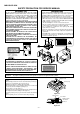
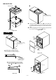
MD-X5H/CP-X5H DISASSEMBLY Caution on Disassembly Whe disassembling the machine or assenbling it after repair, observe the following instructions so as to ensure safety and keep its performance. 1. Unload the compact disc, and mini-disc from machine. 2. Be sure to unplug the power cable before starting disasembly of the machine. 3. When disassenbling each section, remove the nylon band or wire arrangement. If a screw of improper length is fit to the MD mechanism.
MD-X5H/CP-X5H Shield Case (Top Sode) Front Panel (P1) x 1 ø2 x 4mm (K1)x10 ø2.6x10mm (P1) x 1 ø2 x 4mm Display PWB (H1)x4 ø3x10mm (H3)x1 MDMecha Unit (H2)x1 (P1) x 1 ø2 x 4mm CD Holder (J1)x2 ø3x6mm Figure 9-1 Shield Case (Bottom Side) (P1) x 1 ø2 x 4mm (P 1) x 1 ø3 x 10mm (P1) x2 ø3 x 10mm Front Panel Figure 9-5 Jack PWB ( Q2 ) x 1 (L1)x2 ø2.6x10mm Pickup Flexible PWB (*1) Figure 9-2 MD Main PWB ( Q1 ) x 4 ø1.7 x 3mm Pull (M1)x3 ø2.
MD-X5H/CP-X5H 4 MD Mechanism Push the vicinity of end of center decoration notch. Insert the head of screwdriver near 4 , push further the screwdriver, pulling up the net. Thereby the lower pawl is disengaged (at first disengage at one side and then at other side). 6 After disengaging both pawls disengage the upper pawl by the same procedure as stated in 3 above. Figure 10-4 5 (R1)x4 ø1.7x8.9mm Figure 10-1 CP-X5H 1 (A2)x4 ø4x16mm Bottom Side Insert the head of screwdriver or metallic bar (2.
MD-X5H/CP-X5H REMOVING AND REINSTALLING THE MAIN PARTS (A1)x1 ø1.7x5mm MD MECHANISM SECTION Perform steps 1 to 3 of the disassembly method to remove the MD mechanism. How to remove the magnetic head (See Fig. 11-1) Magnetic Head 1. Remove the screws (A1) x 1 pc. Caution: Take utmost care so that the magnetic head is not damaged when it is mounted. MD Mechanism Figure 11-1 Slider Lever How to remove the cartridge holder (See Fig. 11-2) Cartridge Holder Roller Arm Lever 1.
MD-X5H/CP-X5H How to remove the sled motor/loading motor (See Fig. 12-1) 1. Remove the screws (D1) x 1 pcs., and remove the sled motor/loading motor. (D1)x2 Ø1.7x2mm (D1)x2 Ø1.7x2mm Caution: Be careful so that the gear is not damaged. (The damaged gear emits noise during searching.) Loading Motor Sled Motor Figure 12-1 How to remove the spindle motor (See Fig. 12-2) 1. Remove the screws (E1) x 3 pcs., and remove the spidle motor. Caution: Be careful so that the turntable is not damaged.
MD-X5H/CP-X5H CD MECHANISM SECTION Perform steps 1,to 7 and 12 of the disassembly method to remove the CD mechanism. ( A1 ) x2 2.6 x 6 mm How to remove the pickup (See Fig. 13-1) Optical Pickup 1. Remove the screw (A1) x 2 pcs., to remove the shaft (A2) x 1 pc. 2. Remove the stop washer (A3) x 1 pc., to remove the gear (A4) x1 pc. 3. Remove the pickup.
MD-X5H/CP-X5H ADJUSTMENT TUNER SECTION • Setting the Test Mode Holding down the PRE-EQ button and TUNER(BAND) button, press the POWER button. Frequency is set in the memory as shown in Table 19. Call it with the PRESET button for tuner circuit adjustment and check. fL: Low-range frequency fH: High-renge frequency • AM IF/RF AM Signal oscillator Frequency 400 Hz, 30% modulation Adjusting item Adjusting object Adjusting method IF T351 Indication of IF waveform 450 set must be 1,620 kHz.
MD-X5H/CP-X5H CD TEST MODE CD test mode setting Any TEST mode can be set as shown below by pressing several buttons. Holding down TACK UP/CUE and CD PLAY/PAUSE, turn on POWER. Test Mode Function - CD TEST mode Test mode setting Initialization is not executed. CD TEST mode indication button. Open/Close operation is The pickup can be moved with the ( ) or ( ) button.
MD-X5H/CP-X5H RDS 1. RDS Function Function PI PS PTY PTY(31) EON TI (TA) EON-PTY EON-AF TP TA ASPM STATION NAME PTY SEARCH Select and search (18 kind items) by cyclic NEWS-AFFAIRS ------ OTHER M - ALARM - TP - TA STAND-BY MODE EON-TI/PTY With EON-AF ind. ind. Select and stand-by (17 kind items) by cyclic NEWS-AFFAIRS ------ OTHER M - ALARM - TI 2. DISPLAY DISPLAYand andcontrol controlbuttons buttos Information Provided by RDS EON ASPM PTY TI With the MD-X5H, you can watch two types of RDS service.
– 17 – Yes Yes Compare the field strength of current receiving signal. Is receiving signal stronger than signal which has same PI cord and is already memorized to preset memory ahead of this receiving time? Yes Comparing PI cord same or not? between current receiving PI and before PI which is already memorized by ASPM on this time. Yes RDS signal or not? PI—identify If count 2nd OK? If count 1st OK? Yes SD (TUNE) DET out OK? Begin to scan start 87.50 → 108.
MD-X5H/CP-X5H • ASPM SCAN: 87.50MHz → 108.00 MHz. • Only RDS signal is memorized by ASPM because RDS signal has PI code and is suitable and convenient for ASPM operation. ASPM Comparing field strength, only one strongest RDS station is memorized of all stations (repeater relay stations) that have same PI code. f3 P 1 (PI cord) PS 1 (Station Name) f5 P2 PS 2 f4 --- f1 f2 --- Each PI has AF’S list by individually. Exa: P1 has f1, f2, f3 (same PTY).
MD-X5H/CP-X5H EON summary notice for reference 1. EON-TI/PTY 2. EON-TI/PTY 3. EON-TI 4. EON-TI/PTY 5. EON-TI/PTY 6. EON-TI/PTY 7. EON-TI/PTY 8. EON-TI/PTY 9. EON-TI 10. EON-PTY 11. EON-TI/PTY 12. EON-TI/PTY 13. 14. EON-TI/PTY 15. 16. EON-TI/PTY EON stand-by can be set, only when EON ind. lights up. While EON ind. goes out (NO EON STATION), EON stand-by can't be set. If the EON button is pressed, then “NO EON” is indication the display. Even if switch back ON→TN station continue to keep EON stand-by.
MD-X5H/CP-X5H MD SECTION • Note Remove the MD unit for repeir, and after installing it in the set, be dure to reset it and ascertain that reset has been done. Resetting procedure (1) Unplug the AC cord from the socket, and hold down the RESET buttonm provided at the rear side for more than 10 seconds. (2) Once set the TEST MODE (holding down the TEST MODE (X-BASS botton) and botton together, press the POWER button), and then turn off power. 1.
MD-X5H/CP-X5H • Test Mode 1. AUTO pre-adjustment mode • Automatic pre-adjustment is performed. (After adjustment the grating adjustment mode is set.) • The adjustment value is output with the aid of system controller interface. 2. AUTO adjustment mode • Automatic adjustment is performed. • The adjustment value is output with the aid of system controller interface. • Continuous playback is performed. (Error rate indication, jump test) 3.
MD-X5H/CP-X5H 2. AUTO adjustment mode Step No. • Setting Method Remarks Display Step 1 Testmode STOP state [tsm Step 2 Press the CD PLAY button two times. AUTO adjustment menu [AUTO_AJST_] Step 3 Press once the MD PLAY button. The slide moves to the innermost periphery, and automatic adjustment is started. • In case of high reflection disc changes as follows. PEG→HAG •In case of low reflection disc changes as follows. PEG→LAG→GCG→GEG→LAG End of adjustment If adjustment is OK, Step 4.
MD-X5H/CP-X5H 3. RESULT mode (final adjustment) Step No. Step 1 Setting Method Remarks Testmode STOP state Display [tsm RESULT menu e ] Step 2 Press the CD PLAY button four times. Step 3 Press once the MD PLAY button. Indication of set value [_RESULT___] [HAG:__ _ ] Step 4 Press once the CD PLAY button. Indication of set value [HBG:__ _ ] Step 5 Press once the CD PLAY button. Indication of set value [LAG:__ _ ] Step 6 Press once the CD PLAY button.
MD-X5H/CP-X5H • If the VOL UP/VOL DOWN button is pressed during setting indication, the setting increases/decreases, and the new setting is stored in RAM. • If the VOL UP/VOL DOWN button is held down, the setting changes continuously with 100 ms cycle. • If the REC button is pressed, the setting returns step by step excepting the following case.
MD-X5H/CP-X5H Setting Method Step No. Remarks Display Step 9 Press once the CD PLAY button. Comparison level setting in case of FOK generation (when focus is "ON") [FOKLEV f_ ] Step 10 Press once the CD PLAY button. LPF coefficient setting (normal) in case of FOK generation [FOKLPFn_ ] Step 11 Press once the CD PLAY button. LPF coefficient setting in case of FOK generation (when focus is "ON") [FOKLPFf_ ] Step 12 Press once the CD PLAY button.
MD-X5H/CP-X5H Setting Method Step No. Remarks Display Step 18 Press once the CD PLAY button. TCRS comparison level 1 for high reflection [TCRSC1P_ ] Step 19 Press once the CD PLAY button. Comparison level in case of COUT generation (playback) [COTLVp__ ] Step 20 Press once the CD PLAY button. Comparison level in case of COUT generation (pecord) [COTLVr__ ] Step 21 Press once the CD PLAY button.
MD-X5H/CP-X5H e) TEMP setting Setting Method Step No. Remarks Display Step 1 Testmode STOP state [tsm Step 2 Press the CD PLAY button seven times. EEPROM setting menu [E E P R O M _ S E T] Step 3 Press once the MD PLAY button. Focus setting menu [__Focus___] Step 4 Press the CD PLAY button four times. [___Temp___] Step 5 Press once the MD PLAY button. TEMP reference value setting TEMP setting menu Setting Method Step No.
MD-X5H/CP-X5H 8. TEST-PLAY mode Setting Method Step No. Remarks Display Step 1 Testmode STOP state [tsm Step 2 Press the CD [TEST_PLAY_] Step 3 Press once the CD STOP button. ADRES setting (Target address initial value is indicated) Press once the MD PLAY button. While searching, set the search output to "H". To start continuous play, return it to "L".
MD-X5H/CP-X5H 10. INNER mode Setting Method Step No. Remarks Display Step 1 Testmode STOP state Step 2 Press the TRACK EDIT button. [tsm Step 3 Press once the MD PLAY button. INNER switch position measurement (SUBQ address and C1 error are also indicated.) [s Step 4 Press once the MD STOP button. INNER menu [__INNER__] INNER menu e ] [__INNER__] c ] : Adress • • Press the MD STOP button while the INNER menu is displayed, to shift to the TEST mode STOP state. 11. EJECT mode Step No.
MD-X5H/CP-X5H Mechanism Adjustment 1.
MD-X5H/CP-X5H EXPLANATION OF ERROR DISPLAY Error display Corrective action Errors Can't REC • Defect occurred successively 10 times during REC-PLAY. • Check that the disc is free from flaw, dust • As a result of occurrence of defect during REC-PLAY the and fingerprint. recordable cluster became zero. Check whether there is any black spot. • Adress is unreadable. REC state connot be set for 20 seconds Check for disc disalignment and run-out. although retry is repeated.
MD-X5H/CP-X5H Error display Corrective action Errors BLANK MD • UTOC was read but total TNO and the number of characters of • Perform recording to check that the disc is recordable disc. NAME was 0? DEFECT • Focusing error was caused by shock during REC-PLAY. • Check that the disc is free from flaw,dust, fingerprint and black spot. Check for disc disalignment and run-out. TOC W ERROR • Although UTOC can be read but UTOC cannot be rewritten. • Check that the record head contact is normal.
MD-X5H/CP-X5H E2-PROM Data List Slide setting Focus setting Item indication Item indication Setting Setting FG 97 H SLG 35 H FF1 9E H SL2 27 H FF2 E0 H SLDLIM 65 H FZHLEV ED H SLDLEV 16 H FOKLEVn 08 H SLKLVk 55 H FOKLEVf 88 H SLKLVt 3A H FOKLPFn 00 H SLKLVm 55 H FOKLPFf 88 H WAITf 90 H Control setting Item indication Spin setting Item indication SPG Setting 20 SPG—in B8 H H SPG—mid 76 H SPG—out 50 H SP1 10 H SP2 87 H SP3 E3 H SP4 E3
REC REC REC – 34 – Figure 34 REC REC WAITf___ CD PLAY FOKLPFf_ CD PLAY REC REC FOKLPFn_ CD PLAY FOKLEVf_ CD PLAY FOKLEVn_ CD PLAY FZCLEV__ CD PLAY FF2_____ CD PLAY CD PLAY CD PLAY CD PLAY CD PLAY CD PLAY SPDLIM__ WAITm___ CD PLAY COTLVr__ CD PLAY COTLVp__ CD PLAY SLCTm___ CD PLAY SLCTt___ CD PLAY SLCTo___ CD PLAY TDPWt___ CD PLAY CD PLAY REC TDPWo___ SP5_____ REC TRKLVt__ CD PLAY CD PLAY SP4_____ TRKLVo__ SP3_____ REC REC CD PLAY CD PLAY TRBLVt__ REC
MD-X5H/CP-X5H NOTES ON SCHEMATIC DIAGRAM • Resistor: To differentiate the units of resistors, such symbol as K and M are used: the symbol K means 1000 ohm and the symbol M means 1000 kohm and the resistor without any symbol is ohm-type resistor. Besides, the one with “Fusible” is a fuse type. • Capacitor: To indicate the unit of capacitor, a symbol P is used: this symbol P means micro-micro-farad and the unit of the capacitor without such a symbol is microfarad.
Figure 36 BLOCK DIAGRAM (1/4) – 36 – M M903 LOADING MOTOR HEAD UP/DOWN M M902 SLED MOTOR M DIRECT SWITCH SW1952 LEAD INSWITCH SW1953 PLAYSWITCH SW1954 RECSWITCH SW1955 LOADING SWITCH SW1956 WRITE PRO LIGHT RECEIVING SECTION RF LIGHT RECEIVING SECTION ERROR SIGNAL MD Q1251~Q1254 D4.3V MOTOR DRIVER IC1601 MONITOR DIODE LASER DIODE D3.2V D6.5/4.75 ~ 5.25V D3.2V RF SERVO/SIGNAL CONTROL IC1101 D4.
– 37 – Figure 37 BLOCK DIAGRAM (2/4) M M PICK UP IN SW702 M701 SPINDLE MOTOR M702 SLED MOTOR TRACKING COIL FOCUS COIL 24 25 30 31 12 13 6 7 1 2 3 4 14 22 32 8 9 10 11 IC5 M56748FP FOCUS/ TRACKING/ SPIN/ SLIDE/ DRIVER 1 5 +B1 PU-IN SW SL+. SL–. DRF PICK UP IC1 IC2 CL, DAT, SELIAL CONTROL/CE +5V 53 ~ 58 61 20 JP– 50 51 52 53 44 43 40 41 RES. CQCK. COIN SQOUT. RWC. WRQ.
CNP301 AM LOOP ANTENNA 2 1 3 9 12 13 AM ANT. COIL T302 2 6 7 5V 8 7 2 4 2 4 X OUT 12 RDS 3 13 14 7 15 FM 20 20 ICT21 LC72720 Q360 +B4 1 24 22 23 AM IF T351 4 8 9 5 IN GND VCC +B4 22 21 11 13 10 6 10 1 21 MPX PHASE 11 FW303 17 7 VOLTAGE REGULATOR +B4 OUT TO CD SERVO SECTION 8 3 4 5 6 IC302 TC72131 PLL 16 7 12 17 X351 IC303 FM IF DET./FM MPX./AM IF IF LA1832 2 OUT AM OSC 1 OSC. X352 4.5MHz 21 AM RF FMOSC VR351 FM MUTE LEVEL 22 23 AM OSC.
SO801 SPEAKER – – + JK603 HEADPHONES L–CH JK652 DIGITAL2 COAXIAL + UNA651 DIGITAL 1 OPTICAL R–CH MD-X5H/CP-X5H AC POWER SUPPLY CORD AC230V 50Hz C 1 3 1 IC554 NJM4558MF OPE AMP. 5 M IC652 74HCU04 INVERTER 31 32 33 34 T801 POWER TRANSFORMER FAN MOTOR M800 OM–OFF FAN MOTOR SW Q895 Q801 F802 T2.5A L250V 8 F803 T2A L 250V –35V 12 IC904 INVERTER 74HC153P 13 16 –10V IC712 FL Driver IX0069AW 13 14 Q860 Q861 5/6.
MD-X5H/CP-X5H A C342 0.022 0.022 C366 0.001 C367 1/16 R350 2.7K 0.022 C365 STEREO VSM AM IF IN AM LOW CUT GND FM/AM OUT SD 0.022 7 C354 CF352 1 3 AM IF 6 5 C353 33P 0.022 C344 C350 2 C364 4 L341 BALUN D303 1SS133 D304 1SS133 IC LA FM I /FM MP 3 3 C351 0.022 C352 10/16 D 1 2 1 2 18 20 19 21 AM RF IN 5.6K R351 1 CF302 CNP301 AM LOOP ANTENNA 22 FM IF IN AM OSC OUT AM MIX OUT AM OSC IN REG FM AFC D302 1SS133 23 LO F R352 1K 0.
RT36 220K RT35 220K MD-X5H/CP-X5H CT36 0.022 C370 1/50 R354 3.9K CT28 47/10 CT29 0.022 19 18 17 16 CT25 560P NC 9 VSSD T3 T4 T5 8 NC T2 7 SYNC T1 RDS-ID DO FLOUT 6 RT21 100K CT21 47/10 LT21 2.2µH 5 4 CT24 0.022 CT23 10/16 15 14 13 CIN 1 2 3 20 VDDD XIN TP XOUT TP CT27 22P (CH) XT21 4.332MHz R30 1K R29 1K R28 1K VREF SYR MPXIN CE VDDA DI CL VSSA 24 23 22 21 D353 1SS133 R355 3.3K C356 0.001 C355 22P R393 1K Q354 KTC3199GR MUTING C358 1/50 C357 2.2/50 0.
MD-X5H/CP-X5H TO CD SERVO PWB CNP904 P51 10 - H TO TUNER SECTION P40 10 - H A CNS904 1 2 3 4 5 6 7 8 9 CL DI CE 25 10 11 12 S_MUTE AUX_A AUX_B L_MUTE REC_RCH REC_LCH MD_LCH MD_GND MD_RCH CD_RCH CD_A_GND CD_LCH 28 26 27 TO TUN P41 J737 0.23µH R692 22K +B R691 R693 22K 6.8K R694 6.8K R698 1.8K A_10V R697 1.8K B C573 82P R569 18K 0V 0V 0V R565 8.2K 0V 2 3 5 6 0V – + 1 0V + – C576 C574 22/50 82P 10/50 C593 0.022 C591 R566 8.2K C575 22/50 7 4 8 C OPE AMP.
MD-X5H/CP-X5H TO TUNER SECTION P41 10 - D 25 24 23 22 Q423 KTC3199GR R431 5.6K R427 100K TUN_LCH TUN_GND TUN_RCH LINE_R_IN R432 5.6K R428 100K LINE_L_IN LINE_GND 0V 0.7V 0V R430 2.2K 3.4V 0V AUX_IN-R 1/50 1/50 1/50 1/50 C501 C503 C505 C507 1K 1K 1K 1K C407 10/50 4.8V C521 0.15/50 C523 0.15/50 4.8V 4.7V C525 0.1/50 C527 0.22/50 42 4.6V 41 4.5V 40 0V 4.8V C529 0.027(ML) C531 0.015 –B (ML) C533 0.0022(M L) 39 4.7V 38 4.5V 37 4.8V 36 4.6V 35 4.5V C535 0.0047 (ML) 34 4.
MD-X5H/CP-X5H A – R831 10K +B F805 Q880 T630mA 2SD2012 –17.5V L 250V +5V(+6.5V WHILE DISC LOADING) +B 5V R880 C880 R884 10K C882 1/50 68K C884 0.01 5.5V 220/16 R887 2.5V 1 3 150K R881 R883 470 22K R886 2 R889 (1/2W) R888 10K 220K 2.2M C881 0.1 Q871 2SD2012 IC802 NJM431L VOLTAGE REGULATOR C867 0.022 +B +B AUDIO C856 47/25 R866 100 C868 0.022 Q853 2SD468C 6V 10V MD_A C857 0.022 8.5V 6.7V C855 100/16 +B C863 10.5V 47/25 C862 100/16 Q851 2SD2012 F806 T630mA L 250V R862 R861 220 2.
MD-X5H/CP-X5H POWER AMP PWB-B3 ER AMP. C801 4451 C831 47/50 – FR834 4.7 (1/4W) Fusible ! C834 1000/25 FR833 4.7 (1/4W) Fusible ! C897 0.022 +B R832 680 C895 2200/50 L801 0.29µH L802 0.29µH R837 6.8 R830 270 (1/2W) 5 6 C832 7 47/50 + C837 0.1 (ML) C838 0.1 (ML) 3 4 R838 6.8 C833 1000/25 R829 270 (1/2W) C842 0.022 C846 0.022 C845 0.022 + C844 0.022 C848 0.022 C847 0.022 1 2 R836 6.8 – R839 10 R835 6.8 C841 0.022 R839 0.001 R840 0.001 SPEAKER SO801 C843 0.022 + – – + C849 0.
RS CS CLK DATA F DIG11 DIG10 DIG09 DIG08 DIG07 DIG06 DIG05 DIG04 DIG03 DIG02 DIG01 DIG00 1 2 C711 390P 3 C712 390P 2.2V 2.2V 4.7V C713 390P C730 1/50 Figure 46 SCHEMATIC DIAGRAM (7/16) – 46 – 4 5 -35V -33V SEG35 0V SEG34-33V SEG33-33V SEG32-33V SEG31-33V SEG30-33V SEG29-33V SEG28-33V SEG27-33V C732 27P (CH) C731 10/16 1 2 3 4 5 6 7 8 9 10 11 12 13 14 15 16 17 18 19 20 21 22 23 24 25 26 27 28 29 30 31 32 R776 68K 3.0V –33V 4.
MD-X5H/CP-X5H VF1 C744 1/50 BI801 VF2 C745 1/50 C746 1/50 C743 1/50 FILMNT2 FILMNT2 FILMNT2 FILMNT2 49 48 3 TO POWER AMP. PWB 2 CNP801 1 P44 1 - G CNS801 3 2 1 -35V AC3.30V 46 47 R711 1.2K R701 1.2K R703 3.3K R704 2.2K SW705 PRE-EQ R705 3.3K SW706 R706 4.7K R707 8.2K R708 18K SW712 CD PLAY/PAUSE SW731 POWER R731 1.2K R712 1.5K SW713 R732 1.5K R713 12K CD-STOP R733 1.8K SW733 TRACK SW734 CD>MD EDIT SW735 MD-REC R734 2.2K R735 3.
MD-X5H/CP-X5H +B +B + - + - REF REF TH C33 0.001 + - 40 CV- 39 SLOF - SLOF 38 HFL 37 + REF - FE1 REF - 5 OR TES 36 TOFF 35 - R16 1.5K R22 R19 R23 6.8K 39K 1.2K VREF SL+ 31 2.2V SL- 30 2.2V 29 2.5V SLD REF SLEO 28 TGL 34 JP+ 33 0V R33 C32 R34 5.6K 27P 1K R32 56K TP1 HF R35 C31 470 0.0027 0V 4.9V 0V 0V 4.9V 4.9V 0V C53 220P C18 1/50 C16 0.001 R21 56K 2.5V SPO 2.5V 27 SP- 26 2.5V 25 2.5V 24 SPI SPG REF - 2.
MD-X5H/CP-X5H +B R77 1K R46 1K R47 1K C56 100P +B XOUT ERROR COERECT FLAG CONTROL RVDD 41 RCHO 40 VVDD FR VSS EFMO RVSS 39 EFMIN 11 TEST2 CLV+ CLV 12 0V CLV_ DIGITAL SERVO 13 V/P 14 0V HLF 15 SERVO TES COMMAND 0V 16 LVDD 36 MUTEL 35 3.4V Q73 KRA107M +B CD_MUTE 0V 4.8V 32 TEST3 2.4V 0V C2F DOUT 31 29 3.7V C43 100/10 0V CD_5V +B CD_D_OUT CD_D_GND 3.7V R97 5.6K 0.5V 9.3V 0V C93 47/16 R93 2.2 (1/2W)C94 0.
MD-X5H/CP-X5H CD SERVO PWB-C (2/2) A MD PLAYBACK SIGNAL MD RECORD SIGNAL B C920 100P C919 100P 4.8V 24 4.8V 25 C901 0.047 0V CLK 1K 1K DATA 1K SERCH R991 R993 R995 4.7V 4.7V R984 1K 4.8V 4.7V 4.5V 0.2V RS CS R982 1K R933 1K 4.5V 4.7V 4.7V 0V 4.7V 0V 0V 0V 0V 0V 0V 0V 0V CLK RS CS VDD MD-IN WRQ DRF DATA SYN 0V RWC R986 1K 0V SQOUT R988 1K 4.8V R990 1K COIN 4.8V CQCK R992 1K 4.8V RES R994 1K 0V WRQ R996 1K 0V R999 1K DRF 0V 1K PC_IN R976 4.7V PC_OUTR977 100 4.
DIG_IN_B +B C937 1/50 C933 0.022 DIGIIN DIG_GND 4.8V SWITCHING Q910 2SC2412KR 1K DATA SYN WRQ DRF 0V 4.8V R1033 10K R1022 22K TUNER_MUTE 4.8V +B Q902 2SC2412KR DSTB1 0V R1034 10K CCB_CL CCB_DI CCB_DO CCB_CE C930 0.1 +B LOAD_SW R1062 10K MDDATA1 R1036 0V10K R1037 0V10K 0V D905 1SS133 R1038 470K Q903 2SC2412KR P-DOWN R1027 330K C921 0.
MD-X5H/CP-X5H A MAIN PWB-A1 (3/3) D651 1SS133 34 B TO MAIN SECTION P43 12 - B 33 32 D652 1SS133 J_AUX_L_OUT J_AUX_GND J_AUX_R_OUT L655 2.2mmH R653 3.9K R654 3.9K R655 27K 30 29 TO MAIN SECTION P43 12 - B 35 36 37 38 39 J_LINE_L_IN J_LINE_GND J_LINE_R_IN J_PHONO_L_IN J_PHONO_GND J_PHONO_R_IN J_A_10V J_A_–12V PHONO AMP. IC651 NJM4558MF R661 1K C661 2.2/50 R662 C662 1K 2.2/50 1 – + 2 3 7 + – 5 6 8 C663 0.0022 C667 470P C665 0.0082 L661 2.2mmH JK651 C668 470P C671 R671 0.
MD-X5H/CP-X5H JACK PWB - A2 FM SIGNAL CNS907 4 3 2 1 SO601 KEY BOARD BI907 4 3 2 1 P50 1 - F CNP907 TO CD SERVO PWB 1 2 3 4 5 6 D_GND KB_+5V KB_CLK_IN/OUT KB_DATA_IN/OUT D632 ISS133 D631 ISS133 C634 0.022 INPUT LEVEL VR602 6 5 4 3 2 1 J_AUX_IN-L J_AUX_VOL-R J-AUX_VOL-L 7 4 3 2 1 R625 56 J_HP_OUT_L J_HP_GND J_HP_OUT_R J_HP_SW L621 2.2mmH R626 56 C628 0.022 JK603 HEADPHONES BI420 4 3 2 1 CNS420 P43 12 - D CNP420 TO MAIN PWB C625 0.01 C626 0.
MD-X5H/CP-X5H A SYRS SYRD SYWR SYD7 SYD6 SYD5 SYD4 1 R1102 TP1137 560 AIN 29 AOUT BIN BOUT EIN EOUT LOGIC CLOCK DATA DVCC 17 18 19 20 21 22 23 24 25 10 WBO-I TP1136 R1154 22K TP1135 R1153 22K TP1134 R1152 22K TP1133 R1151 22K TP1132 R1150 22K 11 C1211 1 12 13 14 15 16 TP1220 FODRF FODRR TRDRF TRDRR SLDRF SLDRR SPDRF SPDRR R1653 100K R1651 R1657 R1655 R1661 R1659 R1665 17 100K 120K 120K 82K 82K 62K 18 19 20 21 22 23 24 25 R1663 62K SYD7 SYD6 SYD5 SYD4 99 98 SYRS SYRDX SYW
MD-X5H/CP-X5H MD MAIN PWB-D 6 R1211 220 2 3 4 5 R1202 1M R1201 150 XL1201 33.8688MH z C1204 12P(CH) C1205 12P (CH) 61 60 59 58 57 56 TP1273 55 54 53 R1263 10K R1261 10K 52 8 1 2 3 4 5 6 7 8 R1962 220K SBCK TEMON TOTMON C1953 0.47 A9 A3 A2 A1 A0 11 12 14 R1969 C1958 56 0.047 CLOCK GENERATOR C1954 15P (CH) R1963 1.5K R1221 220 10 VDD 16 C1957 REF 100/6.
LT21 RT48 RT49 RT21 QT21 C368 C374 B C R365 E CT23 Q353 R393 ZDT21 C369 R362 C373 C371 C372 E E CT24 1 B C B C X351 CT21 CT22 R361 XT21 ICT21 LT22 12 10 CT43 RT34 RT52 Q354 RT33 R366 24 CT37 RT51 CT36 20 13 15 CT25 CT29 5 CT26 RT53 RT32 CT27 CNW401 RT54 RT29 RT36 RT37 RT35 A RT30 CT28 RT28 RT26 MD-X5H/CP-X5H R364 C357 R363 C358 R368 D353 R354 7 C375 R377 B R367 TO CD SERVO PWB CNP303 P61 7 - D 1 TO POWER AMP PWB R370 P58 3 - A R528 R529 R530 C
C375 C370 R367 VR351 2 4 3 6 5 FE301 FM MUTE LEVEL R380 R385 R383 3 2 1 ZD352 R384 L351 B C E C385 12 13 14 15 16 17 18 19 20 21 22 R376 R387 C391 D351 D352 R360 C387 IC302 11 10 9 8 7 6 5 4 3 2 1 Q371 E C B SO301 ANTENNA TERMINAL C394 C392 C386 CNP301 AM 200P AMTENNA 8 C380 C393 R378 R395 L352 R391 Q361 C395 C396 R392 8 Q360 7 R381 R379 ZD351 R370 D303 D301 R358 L353 C344 C343 C332 C362 1 2 C345 1 C355 RT55 L341 C340 C347 R369 R344 T351 C398 3
MD-X5H/CP-X5H A TO MAIN PWB P56 2 - C TO MAIN PWB P56 2 - D CNS820B CNS810 CNK820A C866 ZD880 D821 C867 Q821 C868 B Q862 3 2 1 R865 Q822 3 2 1 R828 RP881 E C C865 R866 F806 T630mA L 250V C873 R863 R821 3 2 1 C823 CNS870 3 2 1 Q501 B C E Q502 C875 CNP870 C824 R822 2 1 Q895 R896 1 2 B 3 2 1 C870 D822 ZD871 CNP810 C555 Q870 C872 Q871 E C B C E D871 K820A Q865 R895 C876 R872 1 2 3 4 5 6 7 FAN MOTOR M800 R873 POWER AMP PWB - B3 C871 B C862 R832 F805 T630
MD-X5H/CP-X5H SW736 MD-EJECT DISPLAY PWB - B2 R735 SW735 MD-REC R707 R708 R734 R736 R733 R732 SW733 TRACK SW732 MD-MD EDIT R731 SW731 POWER SW734 CD-MD EDIT SW708 MD-STOP SW709 MD-PLAY/ PAUSE 94 48 70 65 75 85 80 FL711 C743 R743 C706 33 64 RX701 60 55 3 35 10 15 20 25 30 32 1 Q706 Q705 3 2 1 3 2 1 3 2 1 C731 Q707 3 2 1 1 15 20 L731 Q708 25 C732 30 C730 FW902 C714 C713 35 R751 R711 40 R753 R755 R757 47 11 CNP902 40 R776 5 C707 P61 9 - B 45 I
MD-X5H/CP-X5H A B R67 R66 R64 R65 R62 R63 40 45 R933 R949 R948 76 75 R991 R995 R1000 R998 R1002 Q910 R1061 55 60 65 70 R993 R941 R940 R1003 49 48 50 51 R934 R982 R984 80 R1062 85 R1004 R921 R996 R999 R78 50 90 R1063 R45 55 95 IC901 1 16 IC904 C936 R61 30 35 32 33 R988 R1001 IC2 5 C924 R87 R70 R86 25 64 60 20 15 10 100 C923 5 CNW93 1 R1020 R1021 R1019 R1016 R1018 R1014 R1011 R1015 R1010 R1009 R1008 R1006 10 R978 R981 R986 R990 R929 R939 45 R994
MD-X5H/CP-X5H P59 7 - D TO DISPLAY PWB P64 2 - C TO PICKUP UNIT FW902 P56 6 - F TO JACK PWB CNS907 CNS1 RD WH GY WH GY WH GY 7 6 5 4 3 2 1 CD SERVO PWB-C (BOTTOM) BI1 R9 7 1 2 3 4 5 6 7 8 9 10 11 CNP902 1 C3 R6 R7 R23 R24 C17 C18 CNS1904 TO MD MAIN PWB P63 8 - A R25 R26 R34 C19 C44 BI2 L1 Q81 D4 D3 B C E Q73 12 11 10 9 8 7 6 5 4 3 2 1 TO POWER AMP PWB CNS904 P57 7 - F CNP904 C71 R71 TO PICKUP UNIT P64 2 - C C81 Q71 C70 R74 R76 R75 1 2 3 1 2 3 4 5 6 7 8 CNS2 R42 1 2 3 Q72
MD-X5H/CP-X5H A P61 8 - G TO CD SERVO PWB CNP901 MD FLEXIBLE PWB (42) L1251 CNP 1902 Q1820 R1456 R1452 R1454 R1458 R1460 R1462 R1464 R1466 L1950 LR190 C1722 C1724 CJ172 C1729 CNP1252 2 1 TO MAGNETIC HEAD C1251 D1251 1 24 Q1251 B D1252 MD MAIN PWB - D (TOP) 1 Q1252 24 C1252 CNS1252 P64 5 - H R1251 1 Q1822 C1425 C1904 C1927 C1958 9 3 C1206 4 10 R1471 50 26 51 45 40 30 35 R1962 8 1 25 R1106 10 70 85 90 1 100 C1202 C1208 C1209 R1210 R1211 RC120 2 9
MD-X5H/CP-X5H 1 2 3 4 P61 9 - F TO CD SERVO PWB 1 CNP908 2 CNS1904A MD MAIN PWB - D (BOTTOM) TP1516 TP1504 TP1502 Q1807 5 R1808 TP1901 C1913 4 TP1505 TP1904 TP1902 TP1515 Q1803 TP1507 TP1255 TP1509 R1422 C1957 R1401 R1404 R1429 C1402 TP1455 R1423 TP1508 TP1456 R1424 TP1911 TP1510 TP1713 TP1278 5 C1423 75 C1401 50 TP1273 24 C1105 TP1114 8 R1426 R1662 C1653 R1656 TP1609 C1650 15 R1658 30 TP1610 C1655 25 R1650 TP1220 C1651 TP1275 8 C1605 C1601 TP1608 TP1
MD-X5H/CP-X5H CD MOTOR PWB-E PICKUP UNIT A + SW702 CNP3 PICKUP IN M702 SLED 6 5 4 3 2 1 TO CD SERVO PWB CNS3 P61 12 - C B + COLOR TABLE BR CNS1 CNS2 RD(R) RED OR ORANGE YL YELLOW GR GREEN TO CD SERVO PWB TO CD SERVO PWB P61 10 - B P61 12 - E SW701 OPEN/CLOSE C M703 LOADING MOTOR M701 SPINDLE BROWN BL BLUE VL VIOLET GY GRAY WH(W) WHITE BK BLACK PK PINK CNS10 BR RD OR YL GR D 1 2 3 4 5 TO CD SERVO PWB CNP10 P61 10 - F MD SLED M902 MD SPINDLE M901 MD LOADING M903
MD-X5H/CP-X5H VOLTAGE (MD MAIN PWB) Q1801 PIN VOLTAGE NO. E 5V C 5V B 43V Q1802 PIN VOLTAGE NO. E 0V C 0V B 0.15V Q1803 PIN VOLTAGE NO. E 0V C 0V B 3.1V Q1807 PIN VOLTAGE NO. E 3.95V C 3.2V B 3.3V Q1820 PIN VOLTAGE NO. E 3.2V C 3.18V B 2.4V Q1821 PIN VOLTAGE NO. E 0V C 0V B 3.08V Q1822 PIN VOLTAGE NO. E 0V C 0V B 0.1V Q1451 PIN VOLTAGE NO. E 0V C 3.18V B 0.1V Q1401 PIN VOLTAGE NO. E 3.2V C 3.2V B 0V Q1402 PIN VOLTAGE NO. E 0V C 0V B 2.3V Q1403 PIN VOLTAGE NO. E 3.18V C 0V B 3.
MD-X5H/CP-X5H WAVEFORMS OF CD CIRCUIT (CD SECTION) STOP FOCUS 1 2 PLAY SERCH 5ms 0.50 V IC1 20 F.E 5ms 5.0 V IC1 54 DRF 7 0.5ms 10.0 V JP- 8 0.5ms 0.50 V JP 9 0.5ms 1.00 V TE CUE 0.5ms 1.00 V HF NORMAL DISC TN0=01 4 0.5ms 5.0 V HFL 1 3 5 0.5ms 5.0 V TES 3 0.5ms 10.0 V JP+ 3 1 3 6 10 20ms 1.00 V SPO 11 20ms 2.00 V CLV+ PLAY 2 REVIEW 0.5ms 1.00 V HF TCD-712 (140mm) TN0=01 4 0.5ms 5.0 V HFL 1 5 0.5ms 5.0 V TES 3 6 50ms 10.0 V JP+ 7 50ms 10.0 V JP- 8 50ms 0.
MD-X5H/CP-X5H WAVEFORMS OF MD CIRCUIT (MD SECTION) PLAY STATE Stopped NORM: 100M S/s CH1 2V DC 10:1 500ns/div Filter SMOOTH OFF BW FULL 1 Offset TP1274 (EFMMON) 1997 / 08 / 04 13:35:24 T CH1 500mV AC 10:1 1 PIT PLAY Stopped NORM: 1M S/s 1997 / 08 / 04 09:30:15 T CH1 CH2 CH3 CH4 T --0.000V 0.000V 0.
MD-X5H/CP-X5H Stopped NORM: 1k S/s CH1 2V DC 10:1 9 CH2 2V DC 10:1 CH3 5V DC 10:1 CH4 5V DC 10:1 1997 / 08 / 04 11:23:12 T CH1 5V DC 10:1 1s/div CH2 5V DC 10:1 CH3 52V DC 10:1 2us/div Filter SMOOTH OFF BW FULL Filter SMOOTH OFF BW FULL TP1216 1 6 PLAY Stopped NORM: 100M S/s 1997 / 08 / 04 14:19:52 T Offset 0.000V 0.000V 0.000V 0.
MD-X5H/CP-X5H TROUBLESHOOTING (CD SECTION) When the CD does not function When the CD section does not operate When the objective lens of the optical pickup is dirty,this section may not operate.Clean the objective lens,and check the playback operation.When this section does not operate even after the above step is taken,check the following items. Remove the cabinet and follow the troubleshooting instructions.
MD-X5H/CP-X5H • The CD operation button operates. Check the FOCUS-HF system. Playback is enabled without disc. Yes Focus search OK Does the pickup move up and down two times? Yes Is the output waveform of IC1 pin 16 (FD) identical with that shown in Figure 70-1? No Check the IC5 to CNP2 and periphery. No Yes 0.5s 0.50 V IC1 16 FD Check the IC1 pin 50 (CLK) line, 4 MHz, and check microcomputer dataon pin 51 (CL), pin 52 (DAT) and pin 53 (CE). 0.5s 0.
MD-X5H/CP-X5H • Check the tracking system. Check the waveform of IC1 pin 7 (TE). The waveform shown in Figure 71 appears. The discless state appears soon. Yes The tracking servo does not operate. Playback is enabled in the TEST mode. Although IL is Yes possible, playback is impossible. Yes Data cannot be read. No Check the periphery from the IC1 pin 8 to pin 15, from IC5 to CNP2. Yes Normal jump is impeded, and top Yes of music number is not found. Check the periphery of IC1 pin 14.
MD-X5H/CP-X5H • Check the VCO-PLL system. Playback operation is performed when disc exists. Yes Although the HF waveform is normal, the TOC data cannot be read. Check the PDD waveform. (Figure 72) No Abnormal Check the IC1 pin 43, pin 44, IC2 pin 3, pin 5, pin 7, pin 10, and pin 11. Stop → Play As VCO frequency is locked at 4.32 MHz, voltage of PDO rises and stabili-zes. 0.5s 1.00 V IC2 3 PDO 2 0.5s 1.
MD-X5H/CP-X5H TROUBLE SHOOTING (MD SECTION) When MD fails to operate If the objective lens of optical pickup is contaminated, MD may fail to operate. At first, clean the objective lens to check playback operation. If MD fails persistently to operate, perform checks as follows. If dust or foreign substance is accumulated on the pickup lens, playback is disturbed and indication of TOC (content of tracks) may be disabled. Before adjusting check that the lens is clean.
MD-X5H/CP-X5H • Disc loading is not normal. Yes Is disc loaded when it is inserted? No Check CNP1601 and SW1956. Is the pin 4 of CNP1601 set to L state? No Yes Is change observed on the pin 23 or 24 of IC1601? Check IC1401. No No Yes Is change observed on the pin 30 or 31 of IC1601? Check CNP1604 and IC1601. No Yes Check CNP1604 and CN1604 Yes Is ejection performed when the MD taking-out button is pressed? No Yes Disc retracts soon after completion of disc ejection. Yes Check CNP1601 and SW1956.
MD-X5H/CP-X5H • Normal playback When it has been confirmed that EEPROM value is normal in the TEST mode Is initialization performed normally when high reflection disc is played back? Does the playback time display advance? No No Check IC1201 Does disc rotate normally? No Is lead-in switch turned on in the TEST mode when the pickup is on the innermost periphery (Is the pin 6 of OC1401 on L level?) No Yes Is an attempt to read repeatedly the TOC section of low reflection disc made? Check SW1953, mecha
MD-X5H/CP-X5H • Record and playback operation Insert the low reflection disc, and after verifying the audio output in the normal mode playback set the record/playback TEST mode Recording from start address cannot be performed. Yes Is RF waveform output to the pin 1 IC1201 or TP1274 when playback is performed after recording? Check whether the disc is record-prohibited.
MD-X5H/CP-X5H • Disc motor fails to run Does waveform appear on the pins 24 and 25 of IC1201 in the TEST mode focus gain coarse adjustment step? No Check soldering joint and parts of pins 24 and 25 of IC1201, and peripheral circuit. No Check soldering joint of PWB of completed IC1601 and CNP1601 disc motor. No Check the soldering joint of pins 20 and 21 of IC1201, IC1601, IC1601, CNS1101. Yes Check the waveform on the pins 22 and 23 of IC1201, check the peripheral parts and soldering joint.
MD-X5H/CP-X5H FUNCTION TABLE OF IC IC901 RH-iX2718AFZZ:System Control Microcomputer(iX2718AF) (1/2) Pin No.
MD-X5H/CP-X5H IC901 RH-iX2718AFZZ:System Control Microcomputer(iX2718AF) (2/2) Port Name Input/Output Pin No.
MD-X5H/CP-X5H IC712 RH-iX0069AWZZ:FL Driver (IX0069AW) Pin No.
MD-X5H/CP-X5H IC1101 VHiiR3R55//-1:RF Signal Control (IR3R55) Pin No. Function Terminal Name 1 RF1 RF signal input terminal 1 Input of RF signal output of pickup 2 RF2 RF signal input terminal 2 Input of RF signal output of pickup 3 RF3 RF signal input terminal 3 Input of RF signal output of pickup 4 RF4 RF signal input terminal 4 Input of RF signal output of pickup 5 REFI Reference voltage amp. input terminal 6 REFO Reference voltage amp.
MD-X5H/CP-X5H IC1201 VHiLR37648/-1:ENDEC/ATRAC (LR37648) (1/2) Pin No. Function Terminal Name Input/Output 1* EFMMON 2 AVCC Output — 3 EFMI Input 4 AGND 5 AIN Input Focus error signal A 6 EIN Input Tracking error signal E 7 TCG Input Track cross signal 8 BIN Input Focus error signal B 9 FIN Input Tracking error signal F — EFM monitor output Analog power EFM signal input from RF amp.
MD-X5H/CP-X5H IC1201 VHiLR37648/-1:ENDEC/ATRAC (LR37648) (2/2) Pin No. Function Terminal Name Input/Output 54 TESO1 Output 55 TESO3 In/Output PLLOSC. Microcomputer extension output port 3 in case of selection 56 TEST4 In/Output EXTCLK. Microcomputer extension output port 4 in case of selection 57 CDDATA In/Output High speed dubbing CD data input. Microcomputer extension output port 5 in case of selection 58 CDLRCK In/Output High speed dubbing CD LR data input.
MD-X5H/CP-X5H IC1401 RX-iX0227AWZZ:MD System Microcomputer (IX0227AW) (1/2) Pin No.
MD-X5H/CP-X5H IC1401 RX-iX0227AWZZ:MD System Microcomputer (IX0227AW) (2/2) Pin No.
MD-X5H/CP-X5H 1 RF2 2 RF3 3 GOUT ATTR EFMAGI EFMAGC AGND AVCC EFMI EFMO RF2-1 ADAGI ADAGC 48 47 46 45 44 43 42 41 40 39 38 37 EFM AGC RESISTOR & SW RF1 POUT IC1101 VHiiR3R55//-1: RF Signal Control (IR3R55) 36 ADIPI 35 ADIPO DIFF 34 NC DIFF RF4 4 REFI 5 REFO 6 RFADD 7 TCGI 8 29 TCGO AIN 9 28 AOUT BIN 10 27 BOUT 33 ADLPFO ADIP AGC 32 22KO 31 22KI BIAS EIN 11 30 WBO HPF LPF 26 EOUT LOGIC 13 14 15 16 17 18 19 20 21 22 23 24 AVCC XSTBY
MD-X5H/CP-X5H PARTS GUIDE MODEL MD-X5H CP-X5H “HOW TO ORDER REPLACEMENT PARTS” To have your order filled promptly and correctly, please furnish the following information. 1. MODEL NUMBER 2. REF. No. 3. PART NO. 4. DESCRIPTION For U.S.A. only Contact your nearest SHARP Parts Distributor to order. For location of SHARP Parts Distributor, Please call Toll-Free; 1-800-BE-SHARP MARK: SPARE PARTS-DELIVERY SECTION Explanation of capacitors/resistors parts codes Capacitors Resistors VCC ....................
MD-X5H/CP-X5H NO.
MD-X5H/CP-X5H NO. L1102 L1201 L1203 L1251 L1601 L1701,1702 L1950 LR190 LT21,22 PRICE RANK PART CODE VPBNNR47K0000 VPBNNR47K0000 VPBNN4R7K0000 VP-NM470K0000 RCILZ0016AWZZ VPBNN100K0000 RCILZ0016AWZZ VPBNN4R7K0000 VP-XH2R2K0000 DESCRIPTION NO. 0.47 µH 0.47 µH 4.7 µH 47 µH 1 µH 10 µH 1 µH 4.7 µH 2.
MD-X5H/CP-X5H NO.
MD-X5H/CP-X5H NO.
MD-X5H/CP-X5H NO.
MD-X5H/CP-X5H NO.
MD-X5H/CP-X5H NO.
MD-X5H/CP-X5H NO.
MD-X5H/CP-X5H MD-X5H 306-2 A 306-1 306 701 306-3 B 704 701 304 302 C 702 702 301 D 303 703 E M701 F 305 M702 305x2 G SW702 H PWB-E 1 2 3 4 Figure 9 CD MECHANISM EXPLODED VIEW 9 –– –– 96 5 6
MD-X5H/CP-X5H MD-X5H 608 16 611 A 35 45 8 12 10 5 B 11 18 609 608 611 CNS1903 29 39 30 C 40 B1 609 13 37 A1 607 B2 41 25 3 9 33 22 21 A2 19 610 D 38 601 610 23 26 601 604 31 37 20 601 SW1956 17 601 607 38 605 607 42 607 E PWB-F 6 SW 1952 SW1955 CFW1901 1 SW1953 SW1954 15 603x2 32 43 7 46 14 F 24 603x2 PWB-A 602 612x4 34 611 602 4 B2 A1 B1 G A2 2 M902 M903 36 611 M901 H 606x3 1 2 3 4 Figure 10 MD MECHANISM EXPLODED VIEW – 10 97 – 5
MD-X5H/CP-X5H MD-X5H 244 258 259 261 A 242 262 241 259 261 619 619 601x3 M800 621 617 614 263 601x4 617 601x2 203 260 MD Mechanism 601x3 B 265 605x7 205 610x10 610x2 215 610x2 606 PWB-B2 207 267 C 202 252 213 214 216 606x2 610x2 608 201 253 218 220 221x2 602x2 613x2 219 232 611 264 254 PWB-C 268 231 223 610x3 238 230 602x2 222 D 211 615x3 611 229 228 233 212 207 E 234 PWB-A2 224 207 605x2 SW701 618x2 225 612 210 620 CD Mechanism 226 M703 606
MD-X5H/CP-X5H CP-X5H A 707 TWEETER SP3, 4 B C1, 2 WOOFER SP1, 2 706 705 C 701 709x6 709x2 SP3, 4 D 704 702 E SP1, 2 709x4 F 710 708 / 711 703 712 G H 1 2 3 4 Figure 12 SPEAKER EXPLODED VIEW – 99 12 – 5 6
MD-X5H/CP-X5H PACKING OF METHOD (FOR UK ONLY) MD-X5H CP-X5H 1. Packing Case 2. Packing Add., Left/Right 3. Polyethylene Bag, Unit 4. Polyethylene Bag, Accessories 5. AM Loop Antenna 6. Operation Manual 7. Polyethylene Bag, AC Power Supply Cord 8. Polyethylene Bag, Operation Manual 9. FM Antenna 10. Remote Control 11. Bar Cord Label SPAKC0576AWZZ SPAKA0149AWZZ SSAKH0024AWZZ 92LBAG1460C1 QANTL0001AWZZ TiNSE0186AWZZ 1. Packing Add., Top/Bottom, Speaker 2. Polyethylene Bag, Speaker 3. Sheet 4.
MD-X5H/CP-X5H —MEMO— 14 –– –– 101
MD-X5H/CP-X5H —MEMO— ––102 15 ––
MD-X5H/CP-X5H —MEMO— 16 –– ––103
MD-X5H/CP-X5H COPYRIGHT © 1997 BY SHARP COPORATION ALL RIGHTS RESERVED. No part of this publication may be reproduced, stored in a retrieval system, or transmitted in any from or by any means, electronic, mechanical, photocopying, recording, or otherwise, without prior written permission of the publisher.