
Specifications
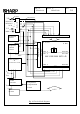

SPEC No.
LC99213A
MODEL No.
LM10V332
PAGE
21
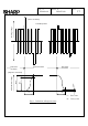
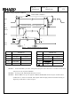
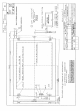
9. Supply voltage sequence condition
1
500 1500ms MIN. (NOTE 1)
a
(
NOTE 2) e
VDD
YD
LP
Interface timing active operation
1
h
XCK
c
(NOTE 3)
f
DATA
DISP
b
1
4.5 V 3.0V
1
3.5 V
2.0V
1
3 V
2.0V
1
3V 1.0V
VDD
VSS d g
Fig.11 Supply voltage sequence condition
(NOTE 1) Power ON/OFF cycle time. All signals and power line shall be in accordance with above
sequence in case of power ON/OFF.
(NOTE 2) In this period, YD and LP shall be “L” level.
(NOTE 3) Before DISP rise up, the signals of YD,LP,XCK,DATA must be input, and the above
condition of “a” must be satisfied. The signals which comply with the interface timing in
Fig.2,Fig.3, and table 7, must be input.
POWER OFF
Symbol Allowable value
e
0 ms MIN. 1 s MAX.
f
0 ms MIN. 1 s MAX.
g
1
10 ms MIN.
1 ms MIN.
-
1
h
1s MIN.
-
POWER ON
Symbol Allowable value
a 0 ms MIN. 1 s MAX.
b
-
100 ns MAX.
c 50 ms MIN. -
d - 10 ms MAX.