MZ-700 SHARP SERVICE MANUAL -r'.............................................................. . CODE: OOZMZ700SM I/E PERSONAL COMPUTER MODEL MZ-700 MZ-1TOl MZ-1POl (FOR THE MZ-lPOI MECHANICAL SECTION REFER TO THE DPG2306 SERVICE MANUAL) INDEX 1. SPECIFICATIONS. . . . . . . . . . . . . . . . . .. . . . . . .. . . . . . .. . . .. . . .. 1 2. NAMES OF FUNCTIONAL COMPONENTS. . . . . . . . . . . . . . . . . . . .. 2 3. SYSTEM BLOCK DIAGRAM .............................. _ .. 3 4.
~\~Z~ 1. 700 SPECIFICATION 1-1. MZ-700 CPU Oock(ct» Memory Video output Screen structure Color designation Music function Timepiece function Keyboard Editing functions Power requirements Temperature Humidity Weight Physical dimensions Sharp LH0080A (Z-80A) 3.
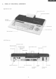
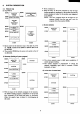
MZ-700 2. NAME OF FUNCTIONAL COMPONENT MZ-700 Front view plolter prioter recorder (cassette) INS. DEL key ":::d'---,----CUrSOI control keV$ Main kev board - - - - - ' MZ-700 Aeer view BrN-Colour switch Channel switch Composi! terminal RF terminal . socket plOHtr printer Dat8 recorder Reset switch !c3S$IIttll) AGe terminal CantUI! re<:order jKk Volume EKt. output terminal Adiust Joy nick ulfminal 1 Ext. printer F,.
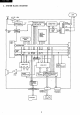
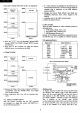
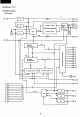
~"q-700 3. SYSTEM BLOCK DIAGRAM F.G A.C. I~ ( sw t t 100V !II -"" ~PO~UP' 0- MEMORY CONTRa. llER (CRTC) 5V PLY CIRCUIT ,.-- ~ eJ Reset sw Fi VIDEO RAM ~~ 1 RESET CIRCUITJ w R.G.B. a:: Cl :Ja:: -.., 00 ...JU oz ~ CHAR GEN I p RF -uw MAIN MEMORY 64KB DRAM ~ a:: .... c( VIDEO ~ MONITOR ROM Z80A CPU III iA ,...... IT \ ADDRESS BUS n A ~dJA H ". ft (ONTROl BUS rn. t\.0 > ~I ?8m r ~ r- t I-I-- ... '-- I-- EMPO CONTROLLER 8255 (PlO) + TEMPO.
4. SYSTEM DESCRIPTION • Boot command: L • With the entry of the boot command L, only the tape loading program is transferred to the system area and the system program is loaded to the system area designated in the DRAM. NOTE: The boot program shown in the figure is the program loaded from the tape and is not the program from the monitor (ROM). 4-1.
~1Z -7CO At the time of manual reset (with I CTRL I in depression) $0000 $0000 MONITOR (ROM) - SYSTEM $1000 $1000 a. 8 x 8 dot characters are displayed on the CRT screen of 40 characters (horizontal) x 25 lines (vertical). Displayed character font is dependent on the 4KB character generator (ROM). b. Manages the monitor ROM, DRAM, video RAM, and peripherals (keyboard, timer, ETC.) mapped to the memory. c. Generates clock to the Z-80A microprocessor. d. Selects the printer I/O port.
To read the contents of a VRAM character, the CPU sends out the relevant address. When RD is forced low, the data is then read via the bidirectional buffer LS245. However, the address range $0000 through $DFFF must be addressed in order to access all the VRAM. This address change is carried out inside the custom LSI with the OUT command described later. Accessing of the VRAM is carried out within the blinking period (BLNK = "H"). If BLNK = "L", then WAIT is applied to the CPU (WA = "L").
\ ,'1Z -700 2) Memory controller In the MZ· 700, it needs to segregate the memory in order to acheive the above mentioned memory mapping. The memory controller is therefore used to perform address management of peripherals assigned to the memory such as DRAM, monitor ROM, video RAM, and keyboard. The bank select method is used to switch memory. Memory selection is acheived using the OUT command.
IV? 7ce 4-4. Memory controller (CRTC) circuit description The memory controller and the CRTC are contained in the single chip custom LSI (M60719). Memory controller signal description & Function IN/OUT Circuit diagram signal name Pin No. Signal name 1 AO l l 16 A15 17 LPH1 IN Clock (17.7MHz) 18 PHI IN CPU clock (3.
CUSTOM LSI < YTl > 1. BLOCK DIAGRAM CRT Control LPHI J I 0 l-{ - I 1/2 r-- 1/2 I.....- I 1/4 IMT COLR NTPL H. SYNC. (PAL) AND ~ "V HBLN ~ ..., ~ LOAD A-C ~ ~ 3 , \. w X w 0.. 8 \ SCREEN POSITION (2) r-- ~ ~ ..J ABC , ~ ~ i= ..J D-K ::> ::i: Y V Cl) Cl) w a: ~ 0 0 "I' 5 V. BLNK CIRCUIT ~ f 3 A4 A5 A6 A7 A8 0 0 0 0 0 0 A9 A10 -0 " / / / P7 P8 pg SYNN 0 - P5 P6 CS DD L--- 9 A3 P3 P4 V. SYNC.
Memory Management (1) IORN A1 A2 A3 A4 A5 AS A7 • ,... " 0 0 0 0 0 PRCN ~ ." -"" " 0 ..... " AO -0 AND 0 BLNK 3 , 2 \. Z WRN '---- 0 LACH 0 ~
Memory Management (2) PH111 ~------------------------------<1SEL CAS circuit WRN MRQN RDN COLR NTSC PAL select 1/4 LPH1 ~-------------In PH 10 NTPL CL 0 GATE 0 VCC 0 0 GND 4-3. Memory mapped I/O ($EOOO - $EOO8) Colour VRAM (VRAM-2) • MZ-700 colour infonnation is managed character by character. One byte of colour infonnation table is assigned to each characters displayed on the TV screen.
a) Signals around the 8255 The 8255 Programmable Peripehral I/O Controller assumes the control of the cassette recorder, CRT screen cursor blinking timing, keyboard scan strobe output, and key return data.
_--464~-__...II.oo ..._ - 4 9 .• 4j.1S----I..-+oI..... 240~-'- 264~'" I " I 1-o . 1 . , I I I , ;.'_ _ _ _ _ __ I CASE1 LONG - - - - -....- - SHORT 368j.1S READ EDGE 368j.1S READ POINT U --J ' READ EDGE READ POINT t (Rising edge starts sampling counter) SHORT (HIGH) 240lls (LOW) 264lls LONG (HIGH) 464lls 494j.1S (LOW) READ POINT 368lls "LONG" is the data written for the bit value of" 1" and "SHORT" for the bit value of "0". Data is read 368~ after the rising edge of the data.
c) Keyboard controDer The 8255 writes strobe (key scan signals) on PA and reads key data from PB. The table shown below is the key map. d) Signals around the 8253 The 8253 Programmable Timer generates the buzzer tone through the counter #(J and keeps the internal timer function via the counters #1 and #2. The counter #(J is used as a square waveform generator (Mode 3). The counter #1 is used as a rate generator (Mode 2) and #2 as an interrupt upon terminal count (Mode 0).
5. DATA RECORDER 5-1. Data recorder (MZ-lT01) Data transfer with the recorder is carried out via the 8255. The read data is sent out through the port Cl and the write data is received through the port C5. The motor on/off control is carried out via the port C3 and that activation of the motor is confmned through the port C4. The signal SENSE goes low when FF, REW, or PLAY pushbutton is pushed on the MZ-} TO I. • Cassette specification Method PWM recording method Rated power 5V ± O.
I iv1Z 700 Troubleshooting procedure Phenomennon CD: Motor and tape do not rotate, when the PLAY button is pushed. Motor fai lure Check if M+ and M·5V are in supply. NO Check if the SW302 interlinked with the P LAY push button is active. Check +5V on REMOTE terminal @. Check the +5V input OV: when SW is on +5V: when SW is off voltage. Check R3009.
Mechanical adjustments RECORD/FAST FORWARDjREWIND torque measurements 1. Set the torque measuring instrument on the cassette tape recorder. 2. Torque value under each mode must be as follows: Position Torque measuring cassette Value PLAYBACK TW-2111 30 '" 70gram·cm FAST FORWARD TW-2231 60 '" 160gram·cm REWIND TW-2231 60 '" 160gram·cm Tape speed adjustment 1. Connect the wow-flutter measuring instrument to :f#!, pin of the CNW3001 connector. 2.
MZ~700 Cassette recorder waveforms Primary stage amplifier output wavefonn Operational amplifier input wavefonn ® CD /1 IJ ~ AWl r vpp Operational amplifier input wavefonn ® 1. 6mv~ pp Tt f1 " " 1 \lV""~'" ov Operational amplifier output wavefonn ® T 1 sVpp 4Vpp Recording input wavefonn (J) - - - Recording signal amplified wavefonn Recording signal amplified wavefonn ® ® T- r ~ O.9V pp 1.SV pp ~ Output wavefonn T 1 1.SVpp T~ 1.
~\;1Z 700 5-2. External recorder playback circuit When the external recorder is used, connection is made with the 8255 by shorting P-12. In this condition, the write data (8255 PC output) is differentiated and sent to the recorder. In the case of read, the signal peak is chopped by DI and D2 (about O.6V), amplified in the 1.2V limiter (about 1.2V), then amplified to 5V in the next stage amplifier.
MZ-700 7. MICRO COlOR GRAPHIC PRINTER 7-1 Micro color graphic printer 1) Block diagram , H \ H J Connectar rr- I-- ~ V-axis stepping motor J I-Drive array I I-- l-l. I-- ~ interfacing Buffer ~ , \ Intelligent - .....
2) Pen exchange method To remove pen, press the pen exchange button, when the slider is at the right handside, push the pen release lever. It is more effective to save power to shut off current while the X and Y axis motors are at a halt. But, there may be a possible malfuction because of unsuppressed vibration, if the current is turned off with a normal pulse width. In order to prevent this, current is applied excessively for more than the given hold time (tMH = 1ms or more).
, MZ--700 [COLOUR PLOTTER PRINTER CONTROL LSI] Pin assignment Name Symbol In/out Function Vss Ground Connected to QV. Vcc Main power Connected to SV. VDD Power Connected to SV. PROG Program Plo - PI 7 Port I Used as printer control signals. P20 - Port 2 Used for data input port from CPU. Do -D 7 Data bus Used for stepper motor control signals. To Test pin Q In Input from pen change switch. Tl Test pin I In Input from paper feed switch.
,Q 700 7-2. Interfacing with the MZ-700 Fig. 1 shows the block diagram for connection with the printer. Fig. 2 shows its circuit description. Fig. 3 shows the timing chart.
MZ-700 8. POWER SUPPLY Power supply circuit description (1) AC source power is rectified through the diode bridge (RB-156). (2) Current flowing through the primary coil of T1 is switched by means of Q 1 so as to induce electromotive force in the secondary coil. To protect voltage fluctuation on the primary side, Q2 is implemented, which will become active to deactivate Ql by dropping the base of Q1 to GND when voltage increase occurs on Q2.
Waveform CD Waveform CID Waveform@ "1 320V -------ov _ _ _ _ _""'lov 2·2. When extremely low output voltage is encountered ( Start I Observe waveform between the collector and emitter of Q1 I I I If Waveform @ If Waveform@ I R5, RS in failure 1 If Waveform(§) I I R9, C12, C", PC1, IC21, C25 in failure Q3 in failure Waveform@ Waveform@ Waveform(§) Unstable waveform - ~ \ Several volts or more ..LI ----~--~----ov 2·3.
~v1Z 2-4. Abnonnal increase of output ripple In case irregular increase is seen for the output ripple like the one below, it needs to replace C22 and C23 with new ones because they have been fatigued. - t 100m V or less t (Normal rippla) Input: AC220 - 240V Output: 5V,3.
9.
74LS174 74LS166 74LS176 I I CLEAR IQ ID CLEAR IQ 74LS273 74LS246 BD 70 I OUTPUT IQ 74LS367A 5A 5Y 4A VCC G2 lA IY 2Y 3A 3Y GND 28 ID 2Q 3Q 2Q GNO
MZ-700 . 10.
C Co.) EXRESET 10- "'0 '0' - .J /0 ICCH LSOO 10r-" C24 1),I/50V "" ~, 220 IK RI07 ,---. 5V "12 IC CH LSOO " I Ti co. LS32 5 • 12~13 LS02 IC6F _ ==-::.. LS32 IC6G IC 6G lS32 RESET 8255 RESET ~,. le7F lSI4 RESET ~- ~RI) 3 --.-----< MREQ 5V --!!...} ./ r.----J f'L-- 10 ~ 1 I lA 18 ICL IQ ICe. ~~,. 5V c •• . 11 IC7F lSI4 1_22.J1/16V III Tantalum IRe", ", 1109 I ,~ ' o f RIOI 10' .5V le 7F LSI4 ------! ----2 ------! ----!.
Co.) ' RO WR .. 0' OB 00 21 07 D OND +5V~VCC ,ooP COOl le BE 8255 • Ao ;'s RESET Ao' 8255 RESET AI AI tiiA II1W c:sEO~CS D. 0, 0' 0, o. 0' >-- O. 0, 20 .. It PA. ~ le 3e P-8 READ C04069 " e "D gill • 0 00 I /0 ~~ 3" P-' 0 L- I~ 0 Ao ~ 06 I .8 le3e e040.9 • le 3e 3.SIC RIO' INTMSK A, D. ~ LSOZ 1C6F iilID 1. 5V oP- '1 l.lI(: c, ",.., HIiJ( 0, JII GNO P-3 P-12 Rill 0.00 I coo Y 5V J1VLT +.v 5. .
~ At , leD. c~ I' r "' "I -I' 5V 0 5V0 5V 0 I' , I' • I I , I I I " D. : 04 : D. "'" , I I I I 5V 0 : D. : 0, : Do , • I I I I I • I I I I I I , I I I I I I I m A, A. A. "4 As A' AT AI I" , , A, 22 "1 I' I' :Wi\ 1>' • Ao A" :==~t':tA~ Ao 2732 IC5H 5v 0 "' "1 le7G $04 < Rn 1>' SEL I' T '0 le7G 504 C "I , V A4 Alz 45 AI! A6 AI4 A1 AI' 5v 0 Iv 0 Tantalum S!fIIIIY ClO IV 0 Ao A. AI A, Az AIO A! All 6 "PT I " W ....... -- .......
Co) Co) eTI iiD Do D, Dz D. I. , ,. 110 III h D,~ A. A, or ~IO I. LJ~~~¥..~.~.~M~.~A'~,J It BA 2016p· I 02 DJ 04 05 01 114 lis ... 111 p, Ill> GT. PlO Ail 5157 All I , ,, 1, ,1"'" Hfi SYN ffj( . p, , P, Aa 23 PlO RESET .V LOAD A,2 A .-0 p,PzP,F'4PsPt;P., 20tc5P-1 Alo I 02 03 04 Os 0. 01' 01 ICAA -CG32 IC6D 7417 sf'......... :1' 6 lSl74 IC 3A ,,>--------' ~ VIO > Vell( RIO( IiIIf ~ le lA LSOO LSOS I EXINT ICTD " IK .V .
.j:lIo c..:I 11 vEl.K 11' SEl RESET CLK SYN 5157 07 ,. --B" p,o p. p, Pr P, '0 P. P, P.---" " ., 7 • 10 12 13 114 III IK ~ s:'OO CL GATE NIP " 120 RFSH ~ t> ill CL GATE CSO SV RAS 17.73 MHz Do 0, 0' o. o. ~ ~ ~ ~ ~ ' WO Z pL!l-0 '---- ViR ~B Ao ;.--.-!l A 5~Wi 4 0 ~ IC5J Rii ~C PRC ~ 5A~~ SV R65 - R80 220 .16 44: abc (not uSed) 23.
w U'I 15 ALPS ASTA 14 FG 25 GND STA 23 13 RDA 21 ARDA 11 12 GND ARDe AIRT 9 10 RDa RD7 ARD7 IRT RD6 13 IS ARD6 7 8 19 GND 12 RD.
IPower unit I Lt:. SOl AC240V A. L' T500mA l.,L}, Z0040 " Cl RBt56 RI 10/2W A\ C7 t~/(OD T I ~ ZOQ74 r%~~~----~--~ " 68 K/2W " 2201C/IW " e l!",F/"OO .2 0' ESIF 5V " ",OOP .22 331( .1." I 3300pF/.. OOV.2 QI •• 10 C2) R21 0 IIJ l000Jj/IO "0 25C31 50 C26 " ." '50 "I G Q2 2SC 12130 '" 0.0:5311 ., VA?I Q3 25CI2130 I/I W ell o. ,~ " ---:~,, le21 TL431C Rn 2.
[Colour encoder circuit] '~f co. '00" IOv le, U/81 • ICICl/SII • • ~U/III .... '" -, .~ ICZ4II4J " " t- 8/W .~, ,C, Cl/4, -, " 0# 2 ... • ...". ,I , • '<3 MCI:S12P 00 ~ • • , . tt- ." '" '" '" I -'OO~ .n ..... " , •" " .'"" .. Cl ..." '00, ." vtt,. M' ff' O~ ... I- I.~ .. ~:7~$O - '" '00 ~/ ...M' ...'" . .~ . , : ~~~ '" ... ... . ' :0 ..'" 2SC~~ ,.. '" k -'" .". -'",. '" '" '" '00, - ::.: '" ~J' 1.1" 'Oy- 0' ~ sw. le I ILF8' "i~ 0' .
[Motor P.W.B. unit] 4 --I\fIIv-- ~ Tri BLK } RED TO MOTOR BLK RED R6 BLUE [A()'IOO2j - MAIN PW8 ". I .~ . .. REAO $""'00 r----- Lf j-!" WRITE ---- .'" 0 [Rot.Sf HEAD -, I1 ~:5005 .ro @ (~2 o::~ @ , ; r~ I~ 'OK 03001 P\.AVBACK ><£40 " II WJ .~OJ u.. ~ .~ RECOROI .- - ~~:~;" •• , nOM 10 " 25C16:52Q 03002"-03004 2SC2021R -l$ i' 1 ... ;;, co? ,,~ " ~o b ,. • I I ;.t :f ~JV fr( 0. • U ~2S046ec le 3001 }lPC 35BC ~ ' -_ _"_,;;""'=TOO _ pwe ...
[Data recorder circuit J o J I H + ~o N I I ~ ~o i.
o .j::o 15P 4P - AIR SEN ARD, GN GN AST ARD ARD ARD 3,; I. 4 23 P" P21 ----.;,...-;- P26 '~- - "':rv~°V-"T ~ :,; Iq Q2 2SC458KC 4 M PI5 - - - - - - : ;31 PI4 PI, 6 INT Ig~ ~===---------~N:C::=3~2~ R3 "---------<~~~T-38 p27 ~--------~~~:=tjr-_-37 IC I ~ To PII PI6 Plo PI2 R9 '" C3 6 LBI'" , I ,3::.;9,---... II SW3 ESET rL.r rlu_- 1'2~8~~_~~~~~~ 27 FEED LPAPE. SWI rr I •J CHANGE SW2 --lI PEN t I 151588 .
MZ-700 PARTS LIST & GUIDE Parts marked with" L1I" is important for maintaining the safety of the set. Be sure to replace these parts with specified ones for maintaining the safety and .performance of the set.
MZ·700 rn CPU Unit Exteriors NO.
MZ·700 rn CPU U~~t Exteriors I I I I ) , 28 7 19 I 20 P ) ~ 2 If /
MZ·700 I2J NO.
MZ·700 IlJ CPU Unit Electronic Components NO.
MZ·700 [3J CPU Unit Electronic Components NO. 81 82 83 84 85 86 87 88 89 90 91 92 93 PARTS CODE VRD-5T2EY391J VRD 5 T 2 E Y 4 3 1 J VRD 5 T 2 E Y 4 7 1 J VRD-5T2EY473J VRD-5T2EY560J VRD-5T2EY561J QACCZ3321QCNI ;I.
MZ-700 [ID Power Supply Unit NO.
MZ..
MZ·700 [1J Key Board Unit NO.
MZ·700 [ID Ca ssette Unit NO.
MZ·700 [ID Cassette Unit NO.
[[] CASSETTE UNIT ~3 4~1 ~. I .
MZ·700 -12-
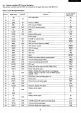
MZ-700 • Index PARTS CODE [C] CCABBI005ACZZ CCABBI006ACZZ CFTACI248AFOl CFTATIOOIACZZ CPNLCI410AFOI CSFTZI00lACZZ [D] DSOCN0344PAZZ DTiP-0098PAZZ DTiP-0099PAZZ DUNT-1150ACZZ DUNT-1151 ACZZ DUNTKI152ACZZ DUNTMI051ACZZ [G] GCABAI006ACZZ GCOVAI364AFSA GCOVHI002ACZZ GFTACI248AFSA GFTARIOl2ACZZ GFTARIOl9ACZZ GFTARI020ACZZ GFTATI007ACZZ GFTATI008ACZZ GiTAU0020AFZZ GLEGGI020CCZZ [H] HBDGBI002ACZZ HBDGDIOOIACZZ HDECZ0063AFSA HPNLCI410AFSA PRICE NEW PART RANK MARK RANK NO.
MZ·700 PARTS CODE QCNW-1048ACZZ QCNW 1049ACZZ QCNW 1051ACZZ QCNW-1733AFZZ QFS-COO02PAZZ QFSHAOO01PAZZ QJAKC1013CCZZ QSOCAOO03PAZZ QSOCZ6424ACZZ QSOCZ6440ACZZ QSW-COO03PAZZ QSW-F0176AFOl QSW-K1013ACZZ QSW-P1009ACZZ QSW-P1010ACZZ QSW-P1011ACZZ QSW S0303AFZZ QSW-S1012ACZZ QSW-S6683RCZZ QTANNOO04PAZZ QTANS1001ACZZ QTANS1002ACZZ [ R] RC-CZ0180PAZZ RC-EZB104AF1H 1/ 1/ RC-EZB105AF1H RC-EZ B106 AF 0 J RC-EZB226AFOJ RC EZT476AFOJ RC QZ0023PAZZ RCRS-1007ACZZ RCRSZ1006ACZZ RH-iX0368PAZZ RH-PX0075PAZZ RHEDA0105AFZZ R
MZ·700 PARTS CODE VRD-S T 2 EE 2 0 5 J VRD-ST2EYIOIJ VRD ST2EYI02J VRD ST2EYI03J 1/ VRD-S T 2E YI 04 J 1/ VRD-ST2EYI21J VRD-ST2EY151J 1/ VRD-ST2EYI52J VRD-ST2EYI53J VRD-S T 2E Y1 8 2 J VRD-ST 2EY 183 J VRD-ST2EY22IJ 1/ VRD ST2EY222J VRD-ST2EY330J VRD-ST2EY33IJ ~T2EY332J 1/ I-VRD-ST2EY391J VRD-ST2EY431J VRD-ST2EY471J 1/ VRD-ST2EY473J VRD-ST2EY560J VRD-ST2EY561J 1/ VRD-ST2EY562J VRD-ST3AF224J VRS-PT3ABIROJ VRS-PT3DB683J VRW-KT3DCI00K VSP0080P-608N VS2SA673-C/-I VS2SB739-C/-l VS2SCI213-DIA VS2SCI652-Q-
MZ-700 SHARP 11-185121\0 71931-100 203 - * 1 S!MMZ700!lT&1POl 250887!720g0700Q SHARP CORPORATION Industrial Instrument Group Reliability & Quality Control Center Yamatokoriyama. Nara 639-11.