UX-A255U SERVICE MANUAL No. 00ZUXA255USME FACSIMILE MODEL UX-A255 SELECTION CODE UX-A255U DESTINATION U.S.A. Chapters 1, 2, 3, 7 and 8 of this manual are omitted because they are partly common to the UX-P100U. Please refer to previous service manual (00ZUXP100USME) for these chapters. CONTENTS CHAPTER 1. GENERAL DESCRIPTION [1] Specifications ............................................ 1-1 [2] Operation panel ......................................... 1-2 [3] Refer to the service manual of UX-P100U.
UX-A255U CAUTION FOR BATTERY REPLACEMENT (Danish) ADVARSEL ! Lithiumbatteri-Eksplosionsfare ved fejlagtig håndtering. Udskiftning må kun ske med batteri af samme fabrikat og type. Levér det brugte batteri tilbage til leverandoren. (English) Caution ! Danger of explosion if battery is incorrectly replaced. Replace only with the same or equivalent type recommended by the equipment manufacturer. Discard used batteries according to manufacturer’s instructions.
UX-A255U CHAPTER 1. GENERAL DESCRIPTION [1] Specifications Automatic dialing: 30 numbers Imaging film: Initial starter roll: (included with machine): 32 ft. (10 m) (approx. 30 letter-size pages) Compatibility: ITU-T (CCITT) G3 mode Input document size: Automatic feeding: Width: 5.8 to 8.5" (148 to 216 mm) Length: 5.5 to 11" (140 to 279 mm) Manual feeding: Width: 5.8 to 8.5" (148 to 216 mm) Length: 5.5 to 23.6" (140 to 600 mm) Effective scanning width: 8.3" (210 mm) max.
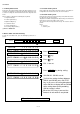
UX-A255U [2] Operation panel 2 1 3 5 4 ABC UP TEL FAX REC/ MEMO 1 PLAY GHI Z A RESOLUTION/ REDIAL RECEPTION MODE STOP COPY/HELP START/MEMORY FUNCTION PQRS 8 9 10 11 12 3 MNO 5 TUV 6 WXYZ 8 9 0 SPEAKER DOWN 7 JKL 7 OpenLCR DEF 2 4 TAD 6 REPEAT SKIP DELETE 13 14 15 16 17 1. Display 10. RESOLUTION / RECEPTION MODE key This displays messages and prompts to help you operate the machine.
UX-A255U [5] Quick setup guide 1 Connect the handset and place it on the handset rest. Note: To enter your name and fax number and set the date and time so that they appear at the top of each fax you send, see pages 16 - 19 of your operation manual. 2 3 Plug the power cord into a 120 V grounded outlet. 4 Connect the telephone line cord to the TEL. LINE jack and a wall telephone jack. Attach the paper tray and document support. TE L INL . E Note: If the support does not go in, turn it over.
;; ;;;; UX-A255U [6] Quick reference guide [7] Option imaging film specifications (UX-5CR) SENDING FAXES Place your document (up to 10 pages) face down in the document feeder. 1. Structure This article is composed of polyester film coated with heat-resistant layer, matt layer and hot melt ink layer, leader film and paper core. Ink film specification is "DNP standard ink film HC". Normal Dialing 1. Lift the handset or press SPEAKER . 2. Dial the fax number. 3.
UX-A255U 3. Settings CHAPTER 2. ADJUSTMENTS (1) Dial mode selector [1] Adjustments DIAL mode (Soft Switch No. SW-B4 DATA No. 3) (step 1) Select "OPTION SETTING". General KEY : Since the following adjustments and settings are provided for this model, make adjustments and/or setup as necessary. DISPLAY: FUNCTION OPTION SETTING (step 2) Select "DIAL MODE". 1. Adjustments of output voltage (FACTORY ONLY) KEY: Push until DIAL MODE indicated because the number of 's changes by the model. 1.
UX-A255U [2] Diagnostics and service soft switch 1. Operating procedure (1) Entering the diagnostic mode Press FUNC → 9 → ROM Ver. TA18 → 8 → # → 7 , and the following display will appear. After 2 sec: DIAG MODE TA18 Then press the START key. Select the desired item with the key or the # key or select with the rapid key. Enter the mode with the START key.
UX-A255U 3. Diagnostic items description 3. 1. Soft switch mode 3. 6. Signal send mode This mode is used to send various signals to the circuit during FAX communication. Every push of START key sends a signal in the following sequence. Moreover, the signal sound is also output to the speaker when the line monitor of the soft switch is on. Used to change the soft switch settings. The soft switch which is stored internally is set by using the keys. The available soft switches are SW-A1 to SW-N3.
UX-A255U 3. 12. Entry data receive 3. 13. Flash memory check In this mode, the registered data sent from the other machine is received and the received data is registered in the machine. When this mode is used for receiving, the other machine must be in the entry data send mode. Data is written into and read from the flash memory to check data conformity. When the unit enters this mode, the check is started. After receiving is completed, the following lists are printed. 1.
UX-A255U 5. Soft switch description • Soft switch SW NO. SW l A1 DATA NO.
UX-A255U SW NO. SW l A6 DATA NO. Switch setting and function ITEM 1 Initial setting 0 1 Reserved 2 End Buzzer Yes No 1 3 Disconnect the line when DIS is received in RX mode No Yes 1 4 5 Equalizer freeze control (MODEM) Equalizer freeze control 7200 BPS only On No Off Yes 0 0 6 7 8 CNG transmission in manual TX mode Reserved Modem speed automatic fallback when RX Yes No Yes No 1 0 0 Remarks 0 level is under -40dBm SW l B1 1 2 3 4 Recall interval 5 Recall times No.
UX-A255U SW NO. DATA NO. 1 Switch setting and function ITEM 1 DTMF signal transmission level (High) 2 SW l B6 No. = Binary input 0 16 8 4 2 1 0 1 2 3 4 5 0 0 1 0 1 1 0 1 3 4 5 6 Dial tone detection (LCR center call) 7 8 Reserved Reserved No Yes 1 2 Light Dark Darker in dark No. 1 No. 2 0 0 Factory setting 1 0 Light 0 1 Dark 1 1 Darker in dark 0 0 No. 3 0 1 0 1 0 No.
UX-A255U SW NO. SW l E1 SW l E2 SW l E3 DATA NO. Switch setting and function ITEM 1 1 Reserved 0 2 3 Reserved Reserved 0 0 4 Reserved 0 5 Reserved 0 6 7 Reserved Reserved 0 0 8 Reserved 0 1 Reserved 0 2 3 Reserved Reserved 0 0 4 Reserved 0 5 Reserved 0 6 7 Reserved Reserved 0 0 8 Reserved 0 1 Reserved 0 2 3 Reserved Reserved 0 0 4 Reserved 0 5 Reserved 0 6 7 Reserved Reserved 0 0 8 Reserved 0 DTMF detection time SW l F1 1 No.
UX-A255U SW NO. SW l G2 SW l G3 DATA NO. Switch setting and function ITEM 1 1 2 Reserved Reserved 0 0 3 4 Reserved Reserved 0 0 5 6 Reserved Reserved 0 0 7 Reserved 0 8 1 2 Reserved Reserved Reserved 0 0 0 3 4 Reserved Reserved 0 0 5 6 Reserved Reserved 0 0 7 Reserved 0 8 Reserved Busy tone detection ON/OFF time (Lower 1 2 duration) No. 1 No. 2 No. 3 No.
UX-A255U SW NO. DATA NO. 1 SW l I2 SW l I3 A.M. quiet detect time Binary input 0 3 4 5 1 0 2 3 4 5 0 1 1 0 1 1 0 6 Reserved 0 7 8 1 2 Reserved Reserved Reserved Max OGM record time 15s 60s 0 0 0 0 3 4 Two way record function Toll saver Disable Disable Enable Enable 0 0 5 6 Reserved Reserved 7 8 Reserved Transfer dial recall 1 AGC maximum gain (line) 3 4 5 2 3 4 5 6 7 8 1 (10 ~ 25 dB) (1 dB step) (10 ~ 25 dB) (1 dB step) Binary input No. = No.
UX-A255U SW NO. SW l J1 DATA NO. Switch setting and function ITEM 1 Reserved 2 Reserved 3 4 Sender’s phone number setting Reserved 5 6 Reserved Summer time setting 1 0 Cannot change Change allowed No Yes 7 No. 7 Off 0 8 No. 8 0 Low 0 Middle 1 High 1 1 1 0 1 0 0 Reserved 0 3 Reserved 0 Low 0 No. 4 5 No. 5 Low 0 0 Middle 1 1 0 1 OPTION 1 0 6 No. 6 Very Low 0 7 No. 7 0 0 1 1 0 1 8 1 No.
UX-A255U SW NO. DATA NO. Switch setting and function ITEM 1 Paper set size 1 2 SW l L2 SW l M1 SW l M2 3 Automatic reduce of receive Print contrast No. 1 LETTER 0 LEGAL 0 A4 1 No. 2 0 1 0 Auto 100 % Lighter Light 0 0 OPTION 0 1 4 No. 4 5 No. 5 0 0 1 1 0 0 6 7 8 0 1 0 1 0 Reception reduction ratio in case of memory ful Reserved No.
UX-A255U SW-A2 No. 8 CNG transmission • Soft switch function description When set to "0" , this model allows CNG transmission by pressing the Start key in the key pad dialing mode. When set to "1", CNG transmission in the key pad dialing mode cannot be performed. In either case. CNG transmission can be performed in the auto dial mode. SW-A1 No. 1 Protect from echo Used to protect from echo in reception. SW-A1 No. 2 Forced 4800BPS reception SW-A3 No. 1, No.
UX-A255U SW-A5 No. 5, No. 6 Digital cable equalizer setting (Reception for Caller ID) SW-B2 No. 7, No. 8 Reserved Set to "0". Line equalization when reception for CALLER ID is to be set according to the line characteristics. Setting should be made according to distance between the telephone and the telephone company central switching station. SW-B3 No. 1 ~ No. 5 Reserved Set to "0". SW-A5 No. 7 Error criterion SW-B3 No. 6, No.
UX-A255U SW-B6 No. 6 Dial tone detection (LCR center call) Used to set YES/NO of dial tone detection (calling LCR center). Phone Number Intended Purpose SW-B6 No. 7, No. 8 Reserved Ring Pattern Set to "0". SW-C1 No. 1, No. 2 Reading slice (Binary) Used to determine the set value of reading density in standard/fine mode. The standard setting is "00" (Factory setting is "00") SW-C1 No. 3, No.
UX-A255U SW-D2 No. 4 Reserved SW-F1 No. 5 ~ No. 8 Remote operation code figure by external TEL (0 ~ 9) Set to "0". Remote operation codes can be changed from 0 through 9. If set to greater than 9, it defaults to 9. The "5 " is not changed. Ex-7 (Default: 5 ) SW-D2 No. 5 Caller ID function Used for Caller ID function. SW-D2 No. 6 Caller ID detect during CI off Detection of caller ID signal is performed as follows: 0:First CI OFF only 1:All of CI OFF SW-F2 No. 1 CNG detection in STAND-BY mode SW-D2 No.
UX-A255U SW-H1 No. 5 Busy tone detect continuation sound detect during OGM SW-I3 No. 3 Two way record function If this switch is set to "1", the machine disables two way recording. Used to detect the continuous tone of specific frequency during OGM output. SW-I3 No. 4 Toll saver Used to turn on the toll saver function. If it is off, the reception frequency in the AM mode is indentical with that in the FAX mode. SW-H1 No.
UX-A255U SW-I7 No. 3, No. 4 AGC slew rate (Mic) SW-L1 No. 8 Reserved The AGC Slew Rate controls the convergence of the message playback level to the desired playback level. A large slew rate will allow faster convergence and a small slew rate will allow slower convergence. Set to "0". SW-L2 No. 1, No. 2 Paper set size At present size of the recording paper. SW-I7 No. 5 ~ No. 8 Reserved SW-L2 No. 3 Automatic reduce of receive If set to 1, it is reduced automatically when receiving. Set to "0".
4–1 LINE HANDSET SPEAKER AMPLIFIER SURGE PROTECT/ FILTER CNPRG CONTROL PWB UNIT CML CI AMPLIFIER FLASH MEMORY 4Mbit TEL/LIU PWB UNIT CLOCK 32.768kHz FLASH ROM 2Mbit TRANSFORMER CLOCK 32.256MHz VBT DRAM 4Mbit PIO FAX MODEM DSP CORE IA(CX20438) CPU RTC S-RAM(32kbit) +3.
4–2 CNLCD CNPN-A 16 CNPN CNCIS CNTH INTERFACE PWB CNPN-A 7 15 16 CNPN CNMT 6 SPEAKER 2 CNSP CONTROL PWB UNIT CNCSW 2 CNPW CNLIUA 6 14 CNLNJ POWER SUPPLY PWB UNIT CNPS CNLIUA TEL/LIU PWB UNIT CNHJ 4 TEL LINE HANDSET AC CORD [2] Wiring diagram OPERATION PANEL PWB NUIT 14 LCD UNIT CONTACT IMAGE SENSOR THERMAL HEAD TX/RX MOTOR CAM SW UX-A255U
UX-A255U [3] Point-to-point diagram CNMT TX/RX MOTOR TPBDTPADTPBD TPAD VMT VMT 1 2 3 4 5 6 THERMAL HEAD VTH VTH STRB1STRB2THI RANK THG THG THG THVDD STRB3STRB4LATCHPCLK DATA VTH 1 2 3 4 5 6 7 8 9 10 11 12 13 14 15 16 CNPN-A KEN4A 1 KEN3A 2 KEN2A 3 KEN1A 4 DG 5 +3.
UX-A255U 3. Operational description CHAPTER 5. CIRCUIT DESCRIPTION Operational descriptions are given below: • [1] Circuit description When a document is loaded in stand-by mode, the state of the document sensor is sensed via the 1 chip fax engine (SCE214V). With depression of the START key in the off-hook state, transmission takes place. Then, the procedure is sent out from the modem and the motor is rotated to move the document down to the scan line.
UX-A255U 4) External RAM and ROM [2] Circuit description of control PWB Moveable and programmble size external SRAM memory of up to 1 MB, DRAM memory of up to 4 MB, and ROM of up to 2 MB can be directly connected to the SCE214V. By using an external address decoder, the size of SRAM and/or ROM can be extened. The ROM stores all the program object code. 1. General description Fig. 2 shows the functional blocks of the control PWB, which is composed of 4 blocks.
UX-A255U 12) Video Processing 20) Power Up/Down Control The CX06835 supports two modes of shading correction for scanner data non-uniformity arising from uneven sensor output or uneven illumination. Corrections are provided on either an 8-pixel group or are applied separately to each pixel. Dark level correction and gamma correction are also provied. Two-dimensional Error Diffusion/Dithering is performed on halftone images.
UX-A255U B) Modem block 4) Features 1) Facsimile Modem • Group 3 facsimile transmission/reception The modem can operate at 14400, 12000, 9600, 7200, 4800, 2400, or 300 bps, and can perform HDLC framing per T.30 at all rates. A programmable DTMF detector, three programmable tone detectors, V.21 Channel 2 FSK 7E flag detector, Caller ID demodulator and ring detector are provided. - ITU-T V.17 and V.33 - ITU-T V.29, V.27 ter, T.30, V.21 Channel 2, T.4 - ITU-T V.17 and V.
UX-A255U 5) Integrated Analog Control Resisters for 20438 The 20438 IA can be used as a Primary Integrated Analog (PIA) codec or as a Secondary Integrated Analog (SIA) codec, depending on the signal connection with the SCE Controller ASIC device. In the SCE100 product, both the PIA and the SIA are packaged external to the SCE Controller device, whereas in the SCE214V, the PIA is packaged with the SCE214V Controller and the SIA is external.
UX-A255U SCE214V (IC3) Terminal descriptions Pin No.
UX-A255U SCE214V (IC3) Terminal descriptions Pin No.
UX-A255U SCE214V (IC3) Terminal descriptions Pin No.
UX-A255U (3) Panel control block The following controls are performed by the SCE214V.
UX-A255U [3] Circuit description of TEL/LIU PWB (1) TEL/LIU block operational description 1) Block diagram TEL/LIU PWB CONTROL PWB RTLOOP MODEM BLOCK (20438 I/A) IC102-B LINE SIGTX H 0,1 0,0 1,0 1,1 SPKRP TXOUT L 0,6dB SIN DAC MIC ENABLE CML SP OUT ENABLE CI DETECTOR SIGRX RXIN MICP PC1 LINEIN IC102-A MIC /LINE SELECT LPF LINE IN ENABLE Q101 0,20,25,30dB Q105 IC101-A ADC RX TEL IN TEL MUTE (H:MUTE) TX LINE OUT ENABLE 0,+4dB LINESEL HANDSET MIC MUTE (H:MUTE) Q102 Q104 IC101
UX-A255U 5. CI detection circuit • CI is detected by the photo coupler which is integrated in series in the primary side TEL circuit well proven in the existing unit. 6. Signal/DTMF transmission level & receiving level • Signal transmission level setting: ATT -8 dB Circuit output: -11 dBm. • DTMF transmission level setting: HF -2.5 dBm Thus, set the level. LF -4.5 dBm 4) Signal selection The following signals are used to control the transmission line of TEL/ FAX signal.
UX-A255U [Signals for status recognition according to input signals] Signal Name Function RHS CI NO Signal Name (CNLIUA) NO Signal Name (CNLIUA) H:The handset is in the on-hook state. 1 RHS- 8 TXOUT L: The handset is in the off-hook state.
UX-A255U [4] Circuit description of power supply PWB 1. Block diagram 2.5A/125V AC IN Noise Filter Circuit Rectifying Smoothing Circuit +24V FUSE 4A/32V Switching Circuit VREG (+5V) Control Circuit Photo Coupler Fig. 7 2-1. Noise filter circuit 2-4. Control circuit The input noise filter section is composed of L1 and C1, which reduces normal mode noise from the AC line and common mode noise to the AC line.
1 2 3 4 5 CNTH-12 CNTH-14 CNTH-13 CNTH-2 CNTH-3 CNTH-10 CNTH-11 CNCIS-4 CNCIS-5 A DG LATCH- DATA PCLK STRB1- STRB2- STRB3- STRB4- ! T CISCLK DG C195 C197 C177 C176 C196 C194 C198 C118 N.M. DG 270 270 270 R175 R173 B 470 RA3 R155 8 7 6 5 270 150 100p/50V x 7 R116 R117 C116 N.M. DG DG N.M. 1M 32.
6–2 1 2 3 4 5 6 A (1-4I) RD- (1-4I) WR- (1-3I) ROMCS- (1-6I) D[7:0] (1-5I) A[18:0] R113 R112 10k +3.3V R125 10k +3.3V 0 Memory block A A0 A1 A2 A3 A4 A5 A6 A7 A8 A9 A10 A11 A12 A13 A14 A15 A16 A17 A18 R115 N.M. B R114 N.M. B IC1 CE WE OE D0 A0 A1 D1 A2 D2 A3 D3 A4 D4 A5 D5 A6 D6 A7 D7 A8 A9 VDD A10 A11 A12 A13 A14 A15 GND A16 A17 N.C.(A18) SST39VF020P FLASH ROM 30 20 19 18 17 16 15 14 13 3 2 31 1 12 4 5 11 10 6 9 7 32 24 8 21 22 23 25 26 27 28 29 C C DG C126 0.
6–3 1 2 3 4 5 6 VTHON A CNLIUA-4 CNDSS-7 CNDSS-6 CNDSS-8 (6-1G) VOLA (6-1G) VOLB (6-1G) VOLC FCSFRDFWRFCLE FALE READY CNPRG-3 CNPRG-1 W-TONE (2-2G) (2-2G) (2-3G) (2-3G) (2-3G) (2-2G) (6-2D) FRSNS(4-3C) (4-4C) ORGSNS(4-5C) DR/RBN (4-6C) CSWI LEDON (5-5E) CNLIUA-16 THCHK CNLIUA-15 (5-3D) (5-5E) CNTH-5 CNLIUA-9 CNLIUA-6 (6-3E) RCVOL (6-3E) DTMFMUTE (6-1A) SIGMUTE (6-1I) SPMUTE CNLIUA-10 CNLIUA-1 CNLIUA-13 CNLIUA-12 CNDSS-5 C190 C203 N.M.
6–4 B 51K R127 DG DG DG DG C PWRDWN- (1-1G) C105 1000p/50V C106 1000p/50V C207 1000p/50V C171 100p/50V FRSNSi(3-3A) ORGSNSi- (3-3A) DR/RBN (3-3A) (3-3A) D CNDSS-3 CNDSS-4 DG E CNPW-4 CNPW-3 CNPW-2 CNPW-1 CNPW-5 CNPW-6 N.M. C158 N.M. R147 MG MG +24V +24V DG <+24V> VREG DG C157 N.M. R170 N.M. DG F CR2032 BAT1 5.6K R109 N.M. C192 0.1u/50V R100 MG G C193 0.1u/50V FG R111 N.M.
1 2 3 4 5 VO A B 0.01u/50V 1000p/50V 0Ω N.M. N.M. C124 0 R192 R1 N.M. DG L100 0 C1 220u/6.3V + 300Ω (2W) R192 0 DYNA ROHM R119 VG R1 +24V +3.3V VG R107 10K B CIS Maker (5-5I) LEDON- CNCIS-1 R120 5.1K C124 VG DG GLED +24V C CNCIS-6 CNCIS-7 CNCIS-2 CNCIS-3 C117 0.1u/50V VG CISVDD C114 0.1u/50V CISVDD 0.
1 2 3 4 5 DSSTX A (3-5A) SIGMUTE CNLIUA-8 (6-6C)TELOUT 10 TXOUT 15 R202 0 R195 DSSRX DSSIN DSSOUT RXIN (1-3I) RLYCONT CNDSS-12 CNDSS-10 CNLIUA-7 CNDSS-13 (6-2F) ICM CNDSS-9 N.M. ZD101 4 B DG C183 3 5 3 C208 DG 4 B DG IC11 DG DG R164 1M C C213 1u/10V-K C179 +3.3V NOT MOUNTED SIGTX B 0 B Q112 C181 C SIGTX (3-3H) D (3-3A) W-TONE DG B Q104 KRC102S Q105 KRC102S B DG NOT MOUNTED C C180 R182 DG DG C 0.1u/16V-K R167 4.
UX-A255U Control PWB parts layout (Top side) 6–7
UX-A255U Control PWB parts layout (Bottom side) 6–8
A B C CNTLJ-5 CNLNJ-1 CNTLJ-2 CNLNJ-6 CNTLJ-4 CNLNJ-2 CNLNJ-3 CNLNJ-4 CNLNJ-5 CNTLJ-3 E E S S EX-T2 T2 L2 N.M. C6 L1 T1 EX-T1 VA1 RA-391P-V6-2 5 ARG AR2 ERZV5D471 L7 N.M. N.M. N.M. N.M. 3 5 10 CML(2/3) 8 N.M. N.C. CML(1/3) OUAZ-SH-124DZ 4 9 C10 0.82 ZD6 N.M. JP22 PC817X4 PC1(1/2) 2 1 D4 1SS133 R117 22K HZ27-A ZD4 L4 C118 JP20 4 NOTE: These marks are all satety-cirtical parts. JP4 N.M.
A B C Vref A CNHJ-3 CNHJ-2 CNLIUA-4 CNHJ-1 CNHJ-4 A (1-1D) (3-5D) C144 1 G Q106 RX– RX+ MICMUTE TX– TX+ S D 5 N.M. Q102 KRC106S N.M. C113 620 C112 2200P 0 R132 C145 C143 0 1 0 C135 L3 N.M. N.M. N.M. JP31 L1 JP30 L2 JP29 R112 1.5K R131 C134 Vref A (3-2A) DG1 1K R124 HSDG Vref B C104 0.1 DG (3-2A) C1 22/50 R130 C119 R127 D2 DG R101 1K + R126 4 DG C101 1000P IN/OUT (1-1D) DG1 R105 R120 C4 22/50 N.M. – (3-2A) N.M.
A B +24VL Vref A DG D3 1SS133 DG R128 R129 5 R123 DG N.M. DG Q103 KRC106S DG DG 2 PC2(2/2) 2 N.M. PC3(2/2) 1 1 Q105 Ci CML HS DG DG CNLIUA-9 CNLIUA-13 CNLIUA-12 Q109 Q107 DG 4 Vref A DPMUTE DPON Vref B N.M. CNLIUA-16 CNLIUA-15 C5 R119 CML(3/3) OUAZ-SH-124DZ PC4(2/2) PC1(2/2) PC817X4 4 3 CNLIUA-17 + +24VA ZD1 R1 SW1 2 1 DG 3 + DG HOOK SW 3 N.M. RLYCNT PH2 0 Q108 100/50 (2-5D) (1-1D) 4 3 C126 C141 C A N.M.
UX-A255U TEL/LIU PWB parts layout (Top side) 6 – 12
UX-A255U TEL/LIU PWB parts layout (Bottom side) 6 – 13
6 – 14 1 2 3 4 5 6 D3 ERA15-06 1 CNAC F1 2.5A/125V 2 A V1 S07K150GA R1 2.2M(1/2W) C1 2.2 L1 19mH/0.5A D2 D4 ERA15-06 ERA15-06 D1 ERA15-06 C28 0.01 C7 0.01 B ZD1 RD27ESAB2 C3 1000P C2 220/200 R10 0.12(1W) R9 47 Q1 FS7KM R3 470K R2 470K [3] Power supply PWB circuit B C27 C26 R8 47K C N.M. C4 1000P C5 0.015 C17 N.M. L2 RS908 D D PC1 PS2501-1L (1/2) R7 180 R6 R5 2.7K C24 270P R4 680 N.M. ZD2 RD4.
UX-A255U Power supply PWB parts layout (Top side) Power supply PWB parts layout (Bottom side) 6 – 15
6 – 16 A B C D CNPN_A-8 CNPN_A-7 CNPN_A-5 CNPN_A-6 CNPN_A-9 CNPN_A-1 CNPN_A-2 CNPN_A-3 CNPN_A-4 FRSNS ORGSNS DG +3.3V E KEN4A KEN3A KEN2A KEN1A 5 CNPN_A-16 CNPN_A-15 CNPN_A-14 CNPN_A-13 CNPN_A-12 CNPN_A-11 CNPN_A-10 SEN6 SEN5 SEN4 SEN3 SEN2 SEN1 SEN0 SW1 SW2 DG + D7 1SS133 D6 1SS133 D1 1SS133 D5 1SS133 D4 1SS133 D3 1SS133 R6 R5 N.M. 3 6 9 # START A 2 5 8 0 UP DOWN REC/MEMO 1 4 7 STOP REDIAL PLAY 3 N.M.
UX-A255U Operation panel PWB parts layout (Top side) Operation panel PWB parts layout (Bottom side) Note: Since the parts of PWB cannot be supplied, change it as a unit.
6 – 18 A B C D CNPN-16 CNPN-15 CNPN-14 CNPN-13 CNPN-12 CNPN-11 CNPN-10 CNPN-9 CNPN-8 CNPN-7 CNPN-6 CNPN-5 CNPN-4 CNPN-3 CNPN-2 CNPN-1 FRSNS SEN4 SEN5 SEN4 SEN5 A SEN6 SEN3 SEN3 SEN6 SEN2 SEN1 SEN1 SEN2 SEN0 SEN0 E FRSNS E ORGSNS +3.3V ORGSNS +3.
UX-A255U PARTS GUIDE MODEL UX-A255 SELECTION CODE UX-A255U DESTINATION U.S.A. CONTENTS 1 Cabinet, etc.
UX-A255U [1] Cabinet,etc.
UX-A255U NO. PARTS CODE PRICE RANK NEW MARK PART RANK DESCRIPTION [1] Cabinet,etc.
UX-A255U [2] Top cover/Sub frame 27 25 16 28 26 15 B1 12 B2 30 6 11 1 B1 20 B2 19 23 13 B2 4 24 29 3 2 B3 24 22 9 PARTS CODE PRICE RANK NEW MARK PART RANK B2 DESCRIPTION [2] Top cover/Sub frame 1 2 3 4 5 6 7 8 9 10 11 12 13 14 15 16 17 18 19 20 21 22 23 24 25 26 27 28 29 30 31 B1 B2 B3 GCOVA2448XHSA MSPRC3301XHZZ NGERP2318XHZZ PGIDM2619XHSA PGIDM2620XHSA LFRM-2227XHZZ LFRM-2232XHZZ MLEVP2363XHZZ MSPRC3305XHZZ MSPRD3302XHZZ NGERH2580XHZZ NGERH2581XHZZ NROLR2483XHZZ NROLR2484XHZZ
UX-A255U [3] Upper cabinet/Document guide upper 901 10 1 9 6 5 13 7 12 15 18 3 4 B1 8 17 11 14 2 16 NO.
UX-A255U [4] Drive unit 1 15 16 4 18 11 8 15 21 14 B1 7 22 20 3 6 9 10 2 12 19 13 5 PARTS CODE NO.
UX-A255U [5] Packing material & Accessories 14 12 2 4 6 21 TAPE TAPE 16 15 3 TAPE 8 11 7 18 AC CORD 9 R 17 5 1 (1) (4) 20 R NO.
UX-A255U NO.
UX-A255U NO.
UX-A255U NO.
UX-A255U NO.
UX-A255U PARTS CODE NO.
UX-A255U Indexx PARTS CODE [C] CCNWN484AXH01 CGERH2314XH04 CGERH2566XH01 CLEVP2358XH01 CLEVP2359XH01 CLEVP2360XH01 CLEVP2361XH01 CLEVP2362XH01 CPAKC292DXH01 CPLTP3183XHR7 CROLR2481XH01 [D] DCEKC282RXHZZ ″ DCEKL364CXH01 ″ DCEKP334CXH05 DCEKP336CXH04 ″ DCEKP337CXH01 ″ DUNTK468BXHFW [G] GCABB2393XHSH GCASP2145XHSB GCOVA2447XHSA GCOVA2448XHSA GLEGG2078XHZZ [H] HPNLH2418XHSD [J] JBTN-2339XHSA JBTN-2340XHSA JBTN-2341XHSA JBTN-2342XHSB [L] LBNDJ2006XHZZ ″ LBSHP2140XHZZ LBSHP2141XHZZ LBSHP2142XHZZ LBSHP2143XHZZ LF
UX-A255U PARTS CODE No.
UX-A255U PARTS CODE 0CBUBC0336AZ/ 0CBUBDBE270C/ 0CBUBDBW5R6C/ 0CBUBDDA300A/ 0CBUBXAD4R3C/ 0CBUBXAD6R2C/ 0CBUBY0020AK/ 0CBUDC0062MZ/ 0CBUDXDAW682/ ″ ″ 0CBUEEB681CT/ 0CBUEEC225CF/ 0CBUEFDR12DB/ 0CBUEXCAP000/ 0CBUEXCAP102/ 0CBUEXCAP103/ 0CBUEXCAP181/ 0CBUEXCAP272/ 0CBUEXCAP332/ 0CBUEXCAP334/ 0CBUEXCAP470/ 0CBUEXCAP472/ 0CBUEXCAP473/ 0CBUEXDAW474/ ″ 0CBUEXJAV332/ 0CBUEZ0666ZZ/ 0CBUFBA222EQ/ 0CBUGA0291ZZ/ 0CBUGA0302ZZ/ 0CBUGA0315ZZ/ 0CBUGCM103BH/ 0CBUGCM103GF/ 0CBUGCS152AC/ 0CBUGCU102JC/ 0CBUGFM224KR/ 0CBUGXGCF
UX-A255U COPYRIGHT © 2001 BY SHARP CORPORATION ALL RIGHTS RESERVED. No part of this publication may be reproduced, stored in a retrieval system, or transmitted in any form or by any means, electronic, mechanical, photocopying, recording, or otherwise, without prior written permission of the publisher. SHARP CORPORATION Communication Systems Group Quality & Reliability Control Center Higashihiroshima, Hiroshima 739-0192, Japan Printed in U.S.A.