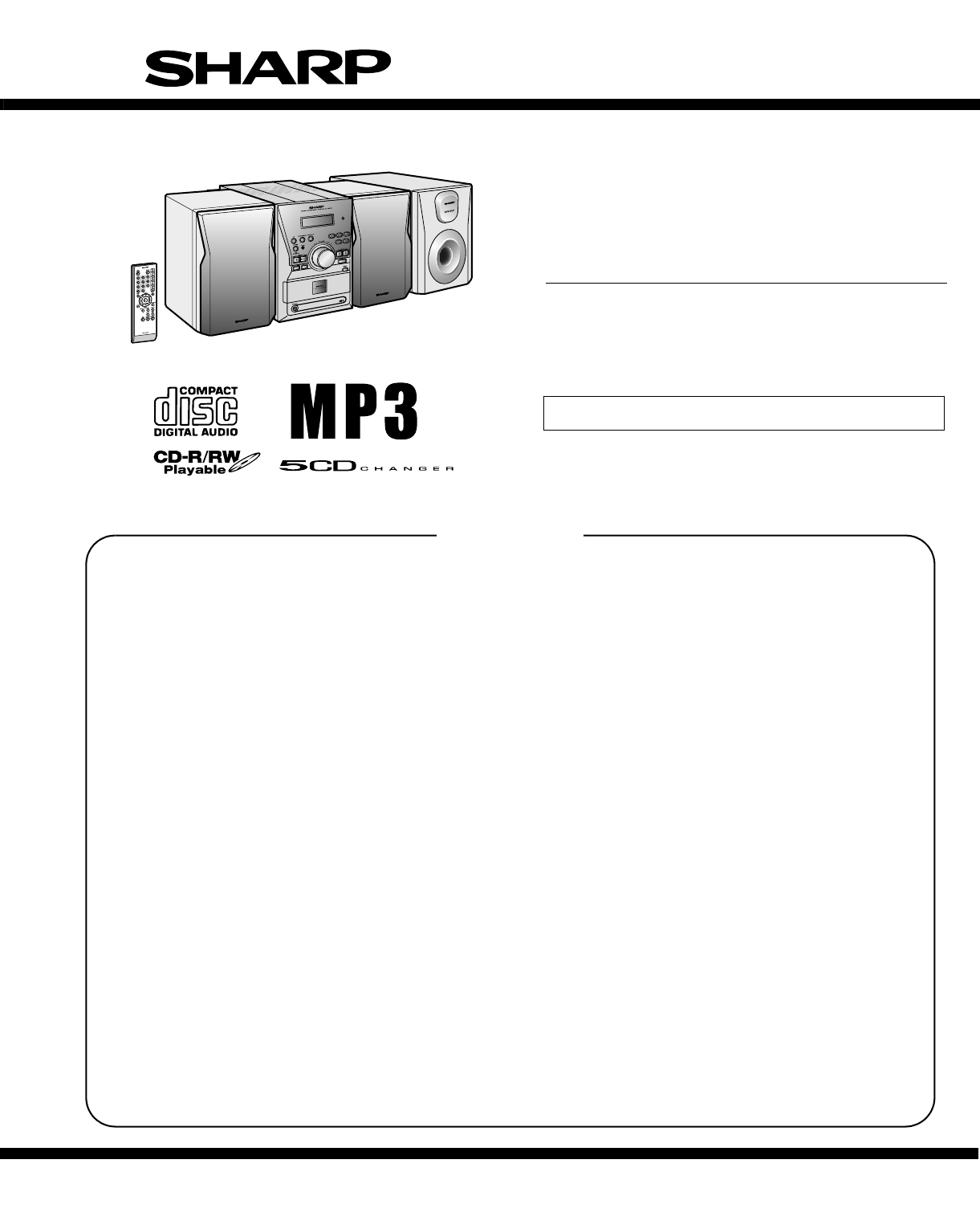
XL-MP60 SERVICE MANUAL No. S2509XLMP60U/ MICRO COMPONENT SYSTEM MODEL XL-MP60 XL-MP60 Micro Component System consisting of XL-MP60 (main unit), CP-MP60F (front speakers) and CP-MP60SW (subwoofer). • In the interests of user-safety the set should be restored to its original condition and only parts identical to those specified be used. CONTENTS CHAPTER 1. GENERAL DESCRIPTION [1] PRECAUTIONS FOR USING LEAD-FREE SOLDER ........................................................
XL-MP60 CHAPTER 1. GENERAL DESCRIPTION XL-MP60 Service Manual [1] PRECAUTIONS FOR USING LEAD-FREE SOLDER 1. Employing lead-free solder "MAIN,TUNER,CD/MP3,DISPLAY,POWER AMP.,JACK,SWITCH" of this model employs lead-free solder. The LF symbol indicates lead-free solder, and is attached on the PWB and service manuals. The alphabetical character following LF shows the type of lead-free solder. Example: Indicates lead-free solder of tin, silver and copper. 2.
XL-MP60 FOR A COMPLETE DESCRIPTION OF THE OPERATION OF THIS UNIT, PLEASE REFER TO THE OPERATION MANUAL. [2] IMPORTANT SERVICE NOTES (FOR U.S.A. ONLY) BEFORE RETURNING THE AUDIO PRODUCT (Fire & Shock Hazard) Before returning the audio product to the user, perform the following safety checks. VTVM AC SCALE 1. Inspect all lead dress to make certain that leads are not pinched or that hardware is not lodged between the chassis and other metal parts in the audio product. 1.5k ohms 10W 2.
XL-MP60 Except for U.S.A ■ General Power source ■ Tuner AC 120 V, 60 Hz Frequency range Dimensions Weight Width: 160 mm (6-5/16") Height: 240 mm (9-7/16") Depth: 319 mm (12-9/16" ) 5.2 kg (11.5 lbs.) ■ Front speaker Front speakers: Maximum input power 75 W Rated input power 37.5 W Impedance 6 ohms Dimensions Width: 165 mm (6-1/2") Height: 240 mm (9-7/16") Depth: 208 mm (8-3/16") 2.2 kg (4.9 lbs.)/each Type ■ Amplifier Output power RMS: 45 W (10 % T.H.D.
XL-MP60 [4] NAMES OF PARTS ■ Front panel 1 2 11 3 12 13 14 15 16 17 4 5 6 7 8 18 9 1. Video/Auxiliary Button 2. Tuner (Band) Button 3. CD Button 4. Power On/Stand-by Button 5. Timer Indicator 6. Disc Stop, Tuning Down Button 7. Disc Play or Repeat, Tuning Up Button 8. Extra Bass/Demo Mode Button 9. Equalizer Mode Select Button 10. Headphone Jack 11. Remote Sensor 12. Disc Number Select Buttons 13. Disc Track Down or Fast Reverse, Tuner Preset Down Button 14.
XL-MP60 ■ Remote control 1 12 2 13 3 14 4 15 5 16 6 17 7 18 8 19 9 20 10 21 1. Remote Control Transmitter 2. Power On/Stand-by Button 3. Direct Track Search Buttons 4. Disc Track Down or Fast Reverse, Tuner Preset Down, Time Down Button 5. Disc Stop Button 6. Extra Bass Button 7. Disc Play or Repeat Button 8. Volume Up and Down Buttons 9. Memory/Set Button 10. Disc Clear Button 11. CD Button 12. MP3/WMA Display Button 13. Disc Number Select Buttons 14.
XL-MP60 CHAPTER 2. ADJUSTMENTS XL-MP60 Service Manual TUNER PWB [1] ADJUSTMENT R311 TP-VT FM BAND COVERAGE fL 1. TUNER SECTION L307 fL: Low-range frequency 36 IC301 • AM IF/RF Signal generator: 400 Hz, 30%, AM modulated Test Stage IF AM Band Coverage AM Tracking Frequency Frequency Display 450 kHz — 1,602 kHz 522 kHz 990 kHz 990 kHz 23 L304 FM RF Instrument Connection Setting/ Adjusting Parts L305 (fL): L306 1.1 ± 0.
XL-MP60 [2] TEST MODE "STOP".............................. "VIDEO/AUX".................... The test mode applied to this microcomputer has three modes, namely the ordinary test mode for adjustment or measurement, the aging test mode, and the self-diagnosis test mode for self-judgment in case of final product inspection. Invalid CLV 2. Step 2 Mode Press the "MEMORY/SET" button in this mode to transmit the laser lighting command LDON (8400) and turn on the laser.
XL-MP60 • 5. Step 5 Mode When the CD initialization operation flow is completed, the mute is turned off, and playback is started. Even if playback reaches the outermost periphery of disc, the operation does not stop. The LCD display indicates the playback passage time as in case of ordinary CD playback. The TUNER TEST 2 mode is obtained with >> + MEMORY/SET + POWER ON/STAND-BY. ->Turn off AC in the TEST 2 mode to restore the initial state. Turn off POWER to protect the memory of TEST 2 mode.
XL-MP60 5. Timer test Mode (TEST 4) 7. Button input diagnosis Test Mode (TEST 6) When this test mode is obtained, the following display lights for one second. When the test mode is obtained, the following is displayed. (STAND-BY AND DEMO OFF STATUS) Set the current time and timer time according to the following procedure to reproduce the timer. This test mode is intended to check whether all the main unit buttons can be detected.
XL-MP60 8. CD MECHANISM Aging Test Mode (TEST 8) OPEN/CLOSE & 5 DISC CHANGER aging test. DISPLAY: FUNCTION: Enter the TEST MODE 8, MCU control the 5 DISC CHANGER OPEN/ CLOSE. After close finished, disc1 to disc5 move in then out for 1 cycle. Then start the next cycle. Request: Every period include 4 operation.
XL-MP60 CHAPTER 3. MECHANICAL DESCRIPTION Home Stereo Service XL-MP60 E Market Manual Service Manual [1] REMOVING AND REINSTALLING THE MAIN PARTS 1. How to remove CD Disc manually (See Fig. 1,2) CD Changer Unit Perform steps 1 to 10 of the disassembly method to remove the CD Changer unit.(see page 3-2,3-3) Arm switch C 1. Rotate the gear cam until the arm switch C becomes the position of the Figure 1. 2. Pull the drawer to the front like the Figure 2. And the CD disc on the carriage is taken out.
XL-MP60 [2] DISASSEMBLY Top Cabinet Caution on Disassembly Follow the below-mentioned notes when disassembling the unit and reassembling it, to keep it safe and ensure excellent performance: 1) Be sure to remove the power supply plug from the wall outlet before starting to disassemble the unit. 2) Take off nylon bands or wire holders where they need to be removed when disassembling the unit. After servicing the unit, be sure to rearrange the leads where they were before disassembling.
XL-MP60 Chassis Transformer Front Panel (G1) x4 ø4x10mm (K1) x3 ø3x8mm (H1) x2 ø3x6mm (K1) x3 ø3x8mm Fan Motor CD Changer Unit Figure 6 (L3) x4 ø3x6mm (J1) x2 ø3x12mm Display PWB CD/MP3 PWB (L2) x1 (J2) x1 (L1) x1 (L2) x1 (J3) x1 Bracket Figure 4 Bracket (L4) x1 ø3x6mm (L4) x1 ø3x6mm Front Panel CD Changer Unit CD Mechanism DVD Changer Unit DVD Tray Cover (N1) x4 ø2.
XL-MP60 -MEMO- 3–4
XL-MP60 CHAPTER 4. DIAGRAMS TO TUNER PWB CNP602 4 4 5 5 7 8 TO CD SERVO PWB CNS407 AUDIO+B +8V M_GND +8V D_GND NC 1 2 3 +B R_CH S/W_CH ÐB D_GND 6 7 +B +12V +B +7V +8V 8 9 CNS602 1 2 3 4 5 A_GND 3 3 6 L_CH 1 2 VEE 1 2 VCC [1] BLOCK DIAGRAM MAIN +B Q101 Q102 CNW602 Q103 +8V Q413 A GND CNP407 Q414 +B DGND +B +B +B +B +B D201 F201 6.3A 125V SO202 AC SOCKET +B +B1 +B 1 F202 6.3A 125V AGND 2 +B C211 ÐB1 D205~D208 F203 1.
GND MUTE3 S/W_RF S/W_IN 12 13 14 15 16 17 18 19 20 21 22 23 24 25 26 27 SO101 SPEAKER TERMINAL S/W_OUT 11 NC MUTE1 10 R_RF GND 9 MUTE2 NC 8 GND VEE 7 NC L_OUT 6 VEE NC 5 R_IN VCC 4 R_OUT NC 3 VCC NC 2 L_IN VEE 1 IC101 LM4781TA POWER AMP.
XL-MP60 [2] BLOCK DIAGRAM TUNER AM BAND COVERAGE fL TO CD DIS CNS3 L306 D305 AM OSC 4 2 5 1 6 CNP302 6 5 4 3 DI CE CL D GND 3 TP-VT +B +12V +B 4 5 D307 FM OSC L307 L302 AM ANT. 6 FM RF BAND PASS FILTER L304 D308 BF301 X301 75KHz 4 5 6 7 8 9 10 11 12 13 14 15 16 17 18 CF302 FM IF FM IF FM FRONT END PLL(TUNER) FM IF DET./FM MPX.
XL-MP60 TO CD DISPLAY PWB CNS302 6 5 4 3 2 1 1 2 3 CD R CD L +B CD_A_GND CNP406 DI CE CL D_GND DO +8V CNP302 TO CD SERVO PWB CNS406 +B DI CE CL TUN R CD R 308 IC602 NJM4558D BUFFER AUX R RSL0 RIN RTRE RBS ROUT VREF VDD CL LSL0 LIN LTRE LBS LOUT VSS CE DI R3 R4 8 7 6 5 4 3 2 1 AUX_R R-CH A_GND L-CH A_GND 12 11 10 9 DO A_GND SO601 VIDEO/AUX IN 13 14 15 16 17 18 19 20 21 22 23 24 L4 4 L3 3 R1 2 +B R2 1 5 L2 + Ð 6 Ð L1 7 IC601 LC75341M AUDIO PROC
XL-MP60 [3] BLOCK DIAGRAM CD/MP3 DISPLAY CD CHANGER PWB ASS'Y TO TUNER PWB CNP406 TO MAIN PWB D_GND SW4 SW3 SW5 SW6 SW2 SW1 SW7 CD_PH2 CD_PH3 MM+ CD_SOL1 MMÐ CD_SOL2 SW8 5 4 AUDIO+B +8V 1 DGND MGND 2 +8V AGND 3 L-CH CNS406 R-CH CNP407 3 2 1 CNS407 Q806 1 2 3 4 5 6 7 8 9 10 11 12 13 14 15 PHOTO INTERRUPTER M MOTOR CONSTANT VOLTAGE SOLENOID Q805 CNP405A CE DI CL DO LRVDD LCHO RCHO 47 46 45 44 43 76 75 RESB 78 7 CD_CL 20 AVSS 6 CD_DI 26 VVSS1 5 CD_DO 37 DVSS 4
XL-MP60 VFD701 FL DISPLAY VF2 40 39 VF1 ~ 37 22 21 ~ 18 14 ~ 4 2 1 CNS101 6 12V 7 P20 63 ~ 52 ~ 50 ~ 47 ~ 51 45 ~ 42 ~ 40 D_GND 30 1 REMOTE SENSOR RX701 IRQ 29 ~ ~ 64 SW1 ~ ~ TIMER_LED M_GND +5.6V +5.6V 1G 5 Q705 11G +5.6V LED701 Ð30V P1 4 P4 D_GND 3.8V VP 3 2 P5 ÐB2 P8 1 P9 TO MAIN PWB CNP101 VF1 VF2 3.
XL-MP60 CHAPTER 5. CIRCUIT DESCRIPTION Home Stereo Service XL-MP60 E Market Manual Service Manual [1] WAVEFORMS OF CD CIRCUIT T Stopped CH1=10 V DC 10:1 1 CH2=1 V DC 10:1 100 ms/div (100 ms/div) NORM:100 kS/s IC801 22 TE 3 2 IC801 16 2 IC801 23 =Filter= Smoothing : ON BW : FULL 1 IC801 22 1 IC801 22 3 IC801 16 5 IC801 25 =Offset= CH1 : 0.0 V CH2 : 0.00 V CH3 : 0.00 V CH4 : 0.
XL-MP60 Stopped CH1=2 V DC 10:1 T 1999/04/07 09:25:28 500 ns/div (500 ns/div) NORM:200 MS/s T 8 IC801 69 1 DOUT =Filter= Smoothing : ON BW : FULL Stopped CH1=2 V DC 10:1 9 =Offset= CH1 : 0.00 V CH2 : 0.00 V CH3 : 0.00 V CH4 : 0.00 V =Record Length= Main : 1K Zoom : 100 T CH2=2 V DC 10:1 CH3=2 V DC 10:1 =Trigger= Mode : NORMAL Type : EDGE CH1 Delay : 2.887 ms Hold off : 0.
XL-MP60 [2] VOLTAGE IC101 PIN NO. 1 2 3 4 5 6 7 8 9 10 11 12 13 14 15 16 17 18 19 20 21 22 23 24 25 26 27 VOLTAGE 30 V -30 V 30 V -30 V 30 V -30 V 0V -30 V 0V 0V -3 V 0V 0V 30 V 0V 0V -30 V 0V 0V -3 V 0V 0V 0V 0V -3 V 0V 0V IC201 PIN NO. 1 2 3 VOLTAGE 10 V 0.6 V 5.6 V IC202 PIN NO. 1 2 3 VOLTAGE 19.8 V 0V 12 V IC203 PIN NO. 1 2 3 VOLTAGE 19.8 V 0V 8V VOLTAGE 1.65 V 1.6 V 1.6 V 1.8 V 1.7 V 1.7 V 1.7 V 1.7 V 1.6 V 1.7 V 1.7 V 2.8 V 1.7 V 1.7 V 1.7 V 1.7 V 1.7 V 3.4 V 0V 0V 3.3 V 1.7 V 1.7 V 1.7 V 1.
XL-MP60 CHAPTER 6. CIRCUIT SCHEMATICS AND PARTS LAYOUT Home Stereo Service XL-MP60 E Market Manual Service Manual [1] NOTES ON SCHEMATIC DIAGRAM • • Resistor: To differentiate the units of resistors, such symbol as K and M are used: the symbol K means 1000 ohm and the symbol M means 1000 kohm and the resistor without any symbol is ohm-type resistor. Besides, the one with “Fusible” is a fuse type.
XL-MP60 [3] SCHEMATIC DIAGRAM MAIN/POWER AMP. POWE A CNW205 B CNS20 CNP20 MAIN PWB-A1 Q101 2HC1815 GR C134 R104 10/16 10K R154 6.8K +B +B +B CNW602 CNS602 R105 10K Q102 TO TUNER PWB A_GND R-CH S/W_CH D_GND +12V +7V +8V 2HC1815 GR CNP602 6-5 12 - G C 1 2 3 4 5 6 7 8 9 1 2 3 4 5 6 7 8 FM SIGNAL L-CH C101 220P R107 C102 2.2K 220P R108 Q103 2.2K 2HC1815 GR R106 10K D C103 220P R109 1K +B +B 3.
XL-MP60 1 2 3 4 5 6 7 8 9 10 11 12 13 14 15 CNS205 1 2 3 4 5 6 7 8 9 NC VEE L_IN S/W_IN 10 11 12 13 14 15 16 17 18 19 S/W_RF 9 MUTE3 GND 8 GND NC 7 NC VEE 6 R_RF L_OUT 5 MUTE2 NC 4 GND VCC 3 R_IN NC R_OUT NC 2 VCC VEE 1 L_RF VCC MUTE1 IC101 LM4781TA POWER AMP. S/W_OUT POWER AMP.
XL-MP60 [4] SCHEMATIC DIAGRAM TUNER A FROM DIS 6-8 2 CNS3 CNP302 B D305 SVC347S R303 100K AM BAND COVERAGE fL L306 C311 560P AM OSC. R304 100K C305 12P(CH) TP-VT C310 27P (UJ) C308 0.018 JR304 0 C348 0.022 R305 100K R311 1K R315 4.7K R310 100K C349 0.0047 C318 0.01 +12V C326 0.1 +B R335 470 C330 22/50 23 22 B01 LP-OUT LP-IN PD AGC AMLOWOUT DET-OUT MPX-IN R-OUT VSS CE DI CL D0 10 11 12 13 14 15 16 17 18 C337 100P (CH) R312 3.
XL-MP60 FROM DISPLAY PWB 6-8 2 - D CNS302 6 5 4 3 2 1 1 2 3 CD L CD R +B CD_A_GND CNP406 DI CE CL D_GND DO +8V CNP302 FROM CD SERVO PWB 6-6 3 - B CNS406 AM SIGNAL FM SIGNAL CD SIGNAL AUX SIGNAL B DI CE CL 1K 1K 1K R603 R602 R601 R622 100K AUX R R621 3.3K C625 10/50 R619 4.7K +B R691 10K TUN R C656 C658 220P C629 10/50 R689 10/50 TUN L C606 10/50 R624 CD L 12K TUN L R620 3.3K 5.6K R647 100K R648 100K R103 1K C618 100/50 C623 0.1 C614 0.1 C616 2.2/16 C610 1/50 C612 0.
XL-MP60 [5] SCHEMATIC DIAGRAM CD/MP3 A CD/MP3 PWB-A3 CNS406 1 1 L-CH L811 1K GND L803 0.82µH R-CH L812 1K R810 100K 2 CNP406 6-2 4 - B TO TUNER PWB B 2 3 3 4 R811 100K SHORT LAND F C 1 FC401 CNP401 1 A D E C809 0.001 C808 0.1 3.3 R812 9.1K 10K R8 3 0.01 0.047 C813 C814 C815 0.056 C816 C817 0.01/25 100/16 C818 0.056 C857 0.022 D C807 100/16 C803 0.1 +B C801 0.1 R804 B C802 33/16 DZH05C2+ Q8 2HC18 C812 0.
XL-MP60 CD SIGNAL C830 0.1 6.8K 6.8K R845 5 7 6 12 100P 100P C822 21 22 23 2425 26 27 28 29 30 31 3233 34 35 36 37 38 39 40 C841 100/16 0.1 VVSS3 2 C847 1.5K 1.5K 1.5K 1.5K 1.5K R844 100K C845 C819 0.1 CNP405A CD_CE 1 CD_RES 2 3 4 CD_DO 5 CD_DI 6 CD_CL 7 R831 R848 R849 R850 R851 R852 C820 0.01 LDS AVSS R828 15K IC801 LC78690 MP3 Decoder DIGITAL SIGNAL PROCESSOR 11 100P 6.
XL-MP60 [6] SCHEMATIC DIAGRAM DISPLAY +B +9V MOTOR DRIVER +5V +B R525 270 (1/2W) L503 0.82µH 1 15 R508A D701 +B +B L707 0.82µH R738 10K R737 10K +B R739 10K R756 10K +B R719 D706 1N4004 CNP405A 6-7 11 - C TO CD SERVO PWB CNP102 6-3 11 - G TO MAIN PWB F 1 1 2 2 3 3 4 4 5 5 6 6 7 7 CNW405 1 2 3 4 5 6 7 1 1 2 3 4 5 6 7 8 2 3 4 5 6 7 CNS102 CD_CE CD_RES R750 R755 R702 R730 +B R701 R706 C701 0.
XL-MP60 Q509 KTC3203 Y 1Y F2 F2 NP P20 P19 P18 P17 P16 P15 P14 P13 P12 P11 P10 P9 P8 P7 P6 P5 P4 P3 P2 P1 NP NP NP 11G 10G 9G 8G 7G 6G 5G 4G 3G 2G 1G NP F1 F1 VFD701 FL DISPLAY 37 36 35 34 33 32 31 30 29 28 27 26 25 24 23 22 21 20 19 18 14 13 12 11 10 9 8 7 6 5 4 2 1 390 40 39 SWITCH PWB-A7 SW717 OPEN/CLOSE 1 2 CNW702B 1 2 CNW702A +B SW8 SW7 SW6 SW5 SW4 SW3 SW2 SW1 P20 P19 P18 P17 P16 P15 P14 P13 P12 P11 P10 P9 VP 71 70 69 68 67 66 65 64 63 62 61 60 59 58 57 56 55 54 53 52 51 P8 50 P7 49 P
XL-MP60 [7] WIRING SIDE OF PWB 1 2 3 4 5 6 7 CNS101 RED LINE DISPLAY PWB-A4 CNW101 1 2 3 4 5 6 7 8 RED LINE 1 2 3 4 5 6 7 8 CNW302 CNS302 6 5 4 3 2 1 7 6 5 4 3 2 1 SWITCH PWB ASS'Y(133) CNS102 RED LINE WH-LINE CNW102 1 2 3 4 5 6 7 SWITCH PWB-A7 2 CNW702B 1 SOLENOID (124) 2 4 6 8 10 12 14 1 3 5 7 9 11 13 15 CNW702A CNP501 2 4 6 8 10 12 14 1 3 5 7 9 11 13 15 CNP405B 1 2 3 4 5 6 7 1 1 2 1 M201(218-4) FAN MOTOR RED FC501 15 15 MOTOR (125) CD CHANGER PWB ASS'Y(132) CNS406 RD BK WH
XL-MP60 TUNER PWB-A2 COLOR TABLE BR 1 2 3 4 5 67 8 CNP602 BROWN 6 5 4 3 2 1 RD(R) RED CNP302 OR ORANGE YL YELLOW GR GREEN BL BLUE VL VIOLET GY GRAY WH(W) WHITE BK BLACK PK PINK CNP301 CNP406 1 2 3 BK RD BK CNS602 WH 8 7 6 5 4 3 2 1 WH RED BK 3 2 1 CNW203 CNP203 RED LINE 1 2 3 7 6 5 4 3 2 1 CNP101 1 2 3 4 5 CNP407 1 2 3 4 5 6 7 BK RD BK CNP103A WH CNP102 9 8 7 6 5 4 3 2 1 CNW602 1 2 3 4 5 6 7 1 2 T201 POWER TRANSFORMER 3 MAIN PWB-A1 YL YL CNP204 RD 4 3 2 1
XL-MP60 [8] WIRING SIDE OF PWB MAIN TOP/POWER AMP./JACK A MAIN PWB-A1 (TOP VIEW) B C AC INPUT SOCKET AC 120V,60Hz CFW101B SO101 SPEAKERS D LEFT FRONT RIGHT E SUB WOOFER F G POWER AMP. PWB-A5 Lead-free solder indication H Lead-free solder is used in there MAIN, POWER, JACK PWB. Refer to "Precautions for handling lead-free solder" for instructions and precautions.
XL-MP60 CFW101A JACK PWB-A6 HEADPHONES 7 8 9 10 Figure 6-13 WIRING SIDE OF PWB (4/12) 6 – 13 11 12
XL-MP60 [9] WIRING SIDE OF PWB MAIN BOTTOM A B C D E F G Lead-free solder indication H Lead-free solder is used in there MAIN, POWER, JACK PWB. Refer to "Precautions for handling lead-free solder" for instructions and precautions.
XL-MP60 MAIN PWB-A1 (BOTTOM VIEW) CHASSIS GND 7 8 9 10 Figure 6-15 WIRING SIDE OF PWB (6/12) 6 – 15 11 12
XL-MP60 [10] WIRING SIDE OF PWB TUNER A TUNER PWB-A2 (TOP VIEW) B TP-VT FM BAND COVERAGE fL C FM RF AM BAND COVERAGE fL D AM IF FROM FM/AM LOOP ANTENNA E AM Tracking LEFT VIDEO/AUX IN RIGHT F G Lead-free solder indication Lead-free solder is used in the TUNER PWB. Refer to "Precautions for handling lead-free solder" for instructions and precautions.
XL-MP60 TUNER PWB-A2 (BOTTOM VIEW) OP A C659 CHASSIS GND X 7 8 9 10 Figure 6-17 WIRING SIDE OF PWB (8/12) 6 – 17 11 12
XL-MP60 [11] WIRING SIDE OF PWB CD/MP3 A B CD/MP3 PWB-A3 (TOP VIEW) C D E F G Lead-free solder indication H Lead-free solder is used in the CD MP3 PWB. Refer to "Precautions for handling lead-free solder" for instructions and precautions.
XL-MP60 WAVEFORM NUMBERS 9 10 11 61 60 8 65 55 70 80 1 75 5 4 50 45 IC1 35 10 30 15 25 3 41 40 6 5 2 12 1 20 21 7 CD/MP3 PWB-A3 (BOTTOM VIEW) 13 12 24 1 The numbers 1 to 12are waveform numbers shown in page 5-1 7 8 9 10 Figure 6-19 WIRING SIDE OF PWB (10/12) 6 – 19 11 12
XL-MP60 [12] WIRING SIDE OF PWB DISPLAY/SWITCH A DISPLAY PWB-A4 (TOP VIEW) B C D E F G SWITCH PWB-A7 Lead-free solder indication H Lead-free solder is used in there DISPLAY,SWITCH PWB. Refer to "Precautions for handling lead-free solder" for instructions and precautions.
XL-MP60 DISPLAY PWB-A4 (BOTTOM VIEW) 7 8 9 10 Figure 6-21 WIRING SIDE OF PWB (12/12) 6 – 21 11 12
XL-MP60 CHAPTER 7. FLOWCHART [1] TROUBLESHOOTING 1. When the CD does not function The CD section may not operate when the objective lens of the optical pickup is dirty. Clean the objective lens, and check the playback operation. When this section does not operate even after the above step is taken, check the following items. Remove the cabinet and follow the trouble shooting instructions.
XL-MP60 (1) Focus-HF system check. Although a CD is inserted and the cover is closed, "NO DISC" is displayed. Press the OPEN/CLOSE switch (SW717) without inserting a disc, and try starting the playback operation. Figure 1 1. Does the pickup move to the PICKUP-IN Switch position? No Sled motor. Yes 2. Does the focus (lens) move up and down? (Waveform drawing Figure 1) No Check the focus peripheral circuit. No Check the laser diode driver Q801 peripheral circuit. No Spindle motor.
XL-MP60 (2) Tracking system check. Check the TE waveform at pin 16 on IC 801. If the waveform shown in Figure 4 appears and soon after NO DISC appears? Yes The tracking servo is not activated. Check the peripheral circuits at pins 15, 16 and 23 on IC801, and FC401. Yes A normal jump operation cannot be completed or the beginning of the track cannot be found. Check the around pin 23 on IC801. No "Initialization" is possible, but play is not possible? No "Initialization" is not possible.
XL-MP60 (4) PLL system check. Stopped CH1=500 mV DC 10:1 When a disc is loaded, start play operation. CH3=1 V DC 10:1 1999/04/05 17:33:17 CH4=1 V 500 ms/div (500 ms/div) DC 10:1 NORM:20 kS/s PDOUT0 3 The HF waveform is normal, but the TOC data cannot be read. 4 PDOUT1 T Check the PDOUT waveform. (Figure 6) FDO 1 CH1 v/DIV 500 mV =Filter= Smoothing : ON BW : FULL Check around pins 26~30 on IC801. =Offset= CH1 : 0.000 V CH2 : 0.0 V CH3 : 0.00 V CH4 : 0.
XL-MP60 CHAPTER 8. OTHERS XL-MP60 Service Manual [1] FUNCTION TABLE OF IC IC402 VHILA6548NH-1: Focus/Tracking/Spin Sled Driver (LA6548NH) Pin No.
XL-MP60 IC402 VHILA6548NH-1: Focus/Tracking/Spin Sled Driver (LA6548NH) MUTE 2 4 VO1+ 5 VO1- 6 (NC) 7 FR (NC) 8 VO2- 9 VO2+ 10 VG2 11 + LEVEL SHIFT VG1 + GND GND 15.4k 12 REG_C 13 REG_B 14 27 VREF 26 VIN4 25 VG4 24 VO4+ 23 VO4- 22 (NC) FR 21 (NC) 20 VO3- 19 VO3+ 18 VG3 17 VIN3 16 CD 15 RESET 15.4k 11k VIN2 VCC2 11k + LEVEL SHIFT 3 28 15.4k 15.
XL-MP60 IC701 RH-iXA033SJZZ: System Microcomputer (IXA033SJ) Pin No.
XL-MP60 Pin No.
1 2 3 4 5 6 7 8 9 10 11 12 13 14 15 16 17 18 19 20 21 22 23 24 25 26 27 28 29 30 S48/PG0 S49/PG1 S50/PG2 S51/PG3 P00 P01 P02 P03 VSS2 VDD2 P04 P05/CKO P06/T6O P07/T7O P10/SO0 P11/SI0/SB0 P12/SCK0 P13/SO1 P14/SI1/SB1 P15/SCK1 P16/T1PWML P17/T1PWMH/BUZ PWM2/INT4/T1IN PWM3/INT4/T1IN P32/INT4/T1IN P33/INT4/T1IN P34/INT5/T1IN P35/INT5/T1IN P36/INT5/T1IN/AN12 P37/INT5/T1IN/AN13 RES XT1/AN10 XT2/AN11 VSS1 CF1 CF2 VDD1 P80/AN0 P81/AN1 P82/AN2 P83/AN3 P84/AN4 P85/AN5 P86/AN6 P87/AN7/MICIN P70/INT0/T0LCP/AN8 P71/IN
XL-MP60 IC801 VHiLC7890/-1: MP3 Decoder Digital Signal Processor (LC78690) Pin No.
XL-MP60 Pin No. 60* 61 62 63 64 65 66 67 68 69* 70* 71 72 73 74 75 76 77 78 79 80 Terminal Name LRSY VVDD2 VPREF2 VCOC2 VPDOUT2 VVSS2 DVDD1.
XL-MP60 AVDD RCHO LRVSS LRVDD LCHO XVDD XIN XOUT XVSS AMUTEB DOUT DVDD DVSS DVDD1.
XL-MP60 [2] FL DISPLAY VFD701 VVK251116//-1 GRID ASSIGNMENT ANODE CONNECTION OUTER DRAWING PIN CONNECTION 8–9
XL-MP60 PARTS GUIDE MICRO COMPONENT SYSTEM MODEL XL-MP60 XL-MP60 Micro Component System consisting of XL-MP60 (main unit), CP-MP60F (front speakers) and CP-MP60SW (subwoofer). CONTENTS [1] INTEGRATED CIRCUITS [10] OTHER CIRCUITRY PARTS [2] TRANSISTORS [11] CHANGER MECHANISM PARTS [3] DIODES [12] CABINET PARTS [4] FILTERS [13] SPEAKER BOX PARTS [5] TRANSFORMERS [14] PACKING PARTS [6] COILS [15] ACCESSORIES [7] VIBRATORS [16] P.W.B.
XL-MP60 NO. PARTS CODE PRICE NEW PART RANK MARK RANK DESCRIPTION [1] INTEGRATED CIRCUITS IC101 IC201 IC202 IC203 IC301 IC402 IC601 IC602 IC701 IC801 VHILM4781TA-1 VHIKIA7805API VHIKIA7812API VHIKIA7808API VHILV23002M-1 VHILA6548NH-1 VHILC75341M-1 VHINJM4558D-1 RH-IXA033SJZZ VHILC78690/-1 AZ AF AE AF AS AL AM AH BF BE Power Amp.,LM4781TA Voltage Regulator,KIA7805API Voltage Regulator,KIA7812API Voltage Regulator,KIA7808API FM FRONT END/PLL (Tuner)/FM IF Det./FM Mpx.
XL-MP60 NO.
XL-MP60 NO.
XL-MP60 NO.
XL-MP60 NO.
XL-MP60 NO.
XL-MP60 NO.
XL-MP60 NO.
XL-MP60 NO.
XL-MP60 [11] CHANGER MECHANISM PARTS A 161 161 114 146 153 139 138 164 164 104 115 B 161 164 165 151 164 169 112 103 109 105 107 C 152 113 148 106 168 108 145 157 D 150 116 141 142 140 144 154 123 110 155 147 158 133 162 165 129 127 159 170 143 156 111 149 E 124 118 130 131 134 167 119 164 126 135 160 117 136 F 120 128 137 125 121 132 101 122 102 164 166 G 163 H 1 2 3 4 11 5 6
XL-MP60 NO.
XL-MP60 [12] CABINET PARTS 208 A 610 604 607 613 238 614 606 B 202 241 603 613 240 606 613 613 232 242 602 242 610 606 227 222 224 610 613 218-3 606 609 218-2 218-4 C 606 237 616 218-1 606 207 606 223 218 606 610 606 610 606 D 239 242 228 242 609 226 606 610 243 235 615 230 225 603 606 201 609 E 219 233 608 231 609 216 234 608 201-1 204 214 233 212 201-3 220 205 608 F 609 608 244 217 221 206 245 215 605 601 604 209 213 G 201-2 211 21
XL-MP60 NO.
XL-MP60 [14] PACKING PARTS PACKING METHOD (FOR U.S.A. ONLY) Setting position of switches and knobs CD Lid CLOSE Polyethylene Bag,Unit SSAKHA040SJZZ Packing Add.,Unit,Left/Right SPAKAA066SJZZ Label,Pop TLABZA076SJZZ Label,UL TLABSA003SJZZ Packing Add.
XL-MP60 NO. PARTS CODE PRICE NEW PART RANK MARK RANK DESCRIPTION [15] ACCESSORIES ! 3 3-1 QACCU0003SJ00 QANTL0009SJZZ TINSEA043SJZZ TINSEA044SJZZ TINSKA006SJZZ RRMCGA029SJSA GCOVAA026SJSA AH AG AE AD AE AP AC AC Power Supply Cord FM/AM Loop Antenna Operation Manual [For U.S.A.] Quick Guide [For U.S.A. Only] Operation Manual [Except for U.S.A.] Remote Control Battery Lid,Remote Control [16] P.W.B. ASSEMBLY (Not Replacement Item) ! PWB-A DCEKKV517SJ03 - Main/Tuner/etc.
XL-MP60 INDEX PARTS CODE [ B B3CPMP60F B3CPMP60SW [ C CFANPA002SJ01 CPNLCA009SJ01 [ D DCEKKV517SJ03 [ G GCABCA004SJSC GCABDA005SJSC GCOVAA026SJSA GCOVAA035SJSA GCOVAA036SJSA GCOVAA039SJSA GEP65X110030 GITARA044SJSA GITARA045SJSA GITASA003SJSC GITASA004SJSC [ H HDECQA092SJSA HDECQA093SJSA [ J JKNBKA010SJSA JKNBZA053SJSA JKNBZA054SJSA JKNBZA055SJSA JKNBZA056SJSA JKNBZA057SJSA JKNBZA058SJSA JKNBZA059SJSA ] [ K KMECZA001SJZZ KRPLE0025SJM2 [ L LANGKA067SJFW LANGKA076SJFW LANGKA086SJFW LANGKA087SJFW LANGKA088
XL-MP60 PARTS CODE " RC-EZD474AF1C RC-EZD476AF1C " RC-EZD477AF1A " " RC-GZA105AF1H " " " " " " " " " " " " RC-GZA106AF1C RC-GZA106AF1H " " " " " " " " " " " " " RC-GZA107AF1H " " " " RC-GZA225AF1C " RC-GZA226AF1H " " " RC-GZA227AF1E RC-GZA334AF1H RC-GZA335AF1C RC-GZA336AF1C RC-GZA475AF1H RC-GZA476AF1H " " " " " " " " " " RC-GZA477AF1C RC-GZV227AF1H RC-GZV337AF1V RC-GZW478AF1V " RC-GZW688AF1E RCILAA002SJZZ RCILBA004SJZZ RCILBA006SJZZ RCILIA001SJZZ RCILRA001SJZZ RCRM-0008SJZZ RCRSPA002SJZZ RCRSPA006SJZZ RCRSP
XL-MP60 PARTS CODE " VCKYCY1EF223Z " " " VCKYCY1EF473Z " " " VCKYCY1HB101K VCKYCY1HB102K " " " " VCKYCY1HB104K " " " " " " " VCKYCY1HB221K " " " " " VCKYCY1HB222K VCKYCY1HB223K VCKYCY1HB332K VCKYCY1HB472K " VCKYCY1HB473K " VCKYCY1HB562K VCKYCY1HF103Z VCKYCY1HF104Z " " " VCKYCY1HF223Z VCKYPA1EF103Z " VCKYPA1HB101K " " VCKYPA1HB102J " VCKYPA1HB104K " " " " " VCKYPA1HB221K VCKYPA1HB272K " VCKYPA1HB331K VCKYPA1HB472K " " VCKYPA1HB561K VCKYPA1HB563K VCKYPA1HF223Z " " " " " " " " VCKYPA1HF473Z " VCQYKA1JM224J VCQ
XL-MP60 PARTS CODE " " " " " " " " " " " " " " " " " " " " " VRD-ST2CD103J " " " " " " " " " VRD-ST2CD104J " " " " " " " " " VRD-ST2CD122J " " " VRD-ST2CD123J " " " VRD-ST2CD152J " VRD-ST2CD153J VRD-ST2CD202J " VRD-ST2CD221J VRD-ST2CD223J " " " " " " VRD-ST2CD272J VRD-ST2CD331J " VRD-ST2CD391J " " VRD-ST2CD392J " VRD-ST2CD471J VRD-ST2CD472J VRD-ST2CD473J VRD-ST2CD561J VRD-ST2CD562J " VRD-ST2CD682J " " " VRD-ST2CD822J " No.
XL-MP60 PARTS CODE " " " " " " " " " " " " VRS-CY1JB104J " " " " " " " VRS-CY1JB106J VRS-CY1JB121J VRS-CY1JB151J VRS-CY1JB152J " " " " VRS-CY1JB183J VRS-CY1JB1R0J " VRS-CY1JB203J VRS-CY1JB221J " " " " VRS-CY1JB222J " " " VRS-CY1JB223J " " " " " " " " " " VRS-CY1JB225J VRS-CY1JB271J " VRS-CY1JB272J " VRS-CY1JB273J " " VRS-CY1JB330J VRS-CY1JB331J " " " " VRS-CY1JB332J " " " " " " VRS-CY1JB391J VRS-CY1JB392J " " " VRS-CY1JB393J " " VRS-CY1JB3R3J No.
XL-MP60 PARTS CODE XJBY930P12000 XJPY930P06000 [ 9 ] 9GD010804727 9GD010814710 9GD010814711 9GD010814712 9GD010814739 9GD010824696 9GD010824717 9GD010824718 9GD010824735 9GD010824736 9GD010824737 9GD010824738 9GD020834262 9GD033004577 9GD033004581 9GD033004584 9GD033004585 9GD450633201 9GD450633202 9GD581194039 9GD582593021 9GD660004091 9GD660824059 9GD660824060 9GD660934072H 9GD660934073H 9GD660934076H 9GD660934077H 9GD660934103H 9GD660934115H 9GD660934117H 9GD660934118H 9GD660934119H 9GD660934120H 9GD6611
XL-MP60 “HOW TO ORDER REPLACEMENT PARTS” To have your order filled promptly and correctly, please furnish the following information. 1. MODEL NUMBER 2. REF. No. 3. PART NO. 4. DESCRIPTION For U.S.A. only Contact your nearest SHARP Parts Distributor to order. For location of SHARP Parts Distributor, Please call Toll-Free; 1-800-BE-SHARP MARK: SPARE PARTS-DELIVERY SECTION Explanation of capacitors/resistors parts codes Capacitors Resistors VCC ....................... Ceramic type VCK ...................
XL-MP60 -MEMO-
XL-MP60 -MEMO-
XL-MP60 COPYRIGHT © 2005 BY SHARP CORPORATION ALL RIGHTS RESERVED. No part of this publication may be reproduced, stored in a retrieval system, or transmitted in any form or by any means, electronic, mechanical, photocopying, recording, or otherwise, without prior written permission of the publisher.