
Specifications
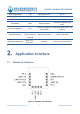
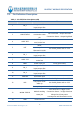
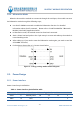
Table Of Contents

DX-BT24-T MODULE SPECIFICATION
Shenzhen DX-SMART Technology Co., Ltd. www.szdx-smart.com
- 3 -
Contents
1.
Introduction ...................................................................................................................................................... - 5 -
1.1. Overview .................................................................................................................................................. - 5 -
1.2. Key Features ............................................................................................................................................- 5 -
1.3. Application .............................................................................................................................................. - 5 -
1.4. Block Diagram ........................................................................................................................................ - 6 -
1.5. Basic Parameters ................................................................................................................................... - 6 -
2.
Application Interface ......................................................................................................................................- 7 -
2.1. Module Pin Definition ..........................................................................................................................- 7 -
2.2. Pin Definition Description...................................................................................................................- 8 -
2.3. Operating Mode ....................................................................................................................................- 9 -
2.4. Energy-saving Mode ............................................................................................................................ - 9 -
2.4.1. Low Power Mode ....................................................................................................................... - 9 -
2.4.2. Hibernation Mode ................................................................................................................... - 10 -
2.5. Power Design ....................................................................................................................................... - 10 -
2.5.1. Power Interface ........................................................................................................................ - 10 -
2.5.2. Power Supply Stability Requirements ............................................................................... - 11 -
2.5.3. Power Down Requirements .................................................................................................. - 11 -
2.5.4. RST Reset Pin Description ..................................................................................................... - 12 -
2.5.5. KEY Pin Definition .................................................................................................................... - 13 -
2.6. Hardware Physical Interface .............................................................................................................- 14 -
2.6.1. UART Interface ..........................................................................................................................- 14 -
2.6.2. Universal Digital IO Port........................................................................................................ - 15 -
2.6.3. I2C Interface .............................................................................................................................. - 15 -
2.6.4. SPI Interface ...............................................................................................................................- 16 -
2.6.5. Analog-to-digital Converter(ADC) ................................................................................ - 16 -
2.7. Reference Connection Circuit ..........................................................................................................- 17 -
3. Electrical Characteristics & Reliability ..................................................................................................... - 18 -
3.1. Maximum Rating ................................................................................................................................. - 18 -
3.2. Working And Storage Temperature .............................................................................................. - 18 -
3.3. Power Consumption ...........................................................................................................................- 19 -
3.4. RF Characteristics ................................................................................................................................ - 19 -
3.5. Static Protection .................................................................................................................................. - 19 -
4. Mechanical Size And Layout Recommendations .................................................................................- 20 -
4.1. Module Mechanical Size................................................................................................................... - 20 -
4.2. Recommend Encapsulation ..............................................................................................................- 21 -
4.3. Module Top View & Bottom View ................................................................................................. - 21 -
4.4. Hardware Design Layout Recommendations ............................................................................. - 22 -
5. Patch Requirements......................................................................................................................................- 23 -
5.1. Storage Conditions .............................................................................................................................- 23 -
5.2. Module Baking Treatment ................................................................................................................- 23 -