DX-BT24 MODULE SPECIFICATION Version:2.
DX-BT24 MODULE SPECIFICATION Update record Version Date V2.1 2018/10/1 V2.2 2020/8/5 Illustrate initial version Author DL Optimize the amount of data Update frequency offset parameters DL V2.3 2020/10/30 Modify the reset pin from high level reset to low level reset DL V2.4 2020/11/30 Correct the description error of the pin function DL V2.5 2022/01/05 new version DL Contact Us Shenzhen DX-SMART Technology Co., Ltd. Email:sales@szdx-smart.com Tel:0755-29978125 Web:www.szdx-smart.
DX-BT24 MODULE SPECIFICATION Contents 1. Introduction.......................................................................................................................................................- 6 1.1. Overview...................................................................................................................................................- 6 1.2. Key Features...........................................................................................................................
DX-BT24 MODULE SPECIFICATION 5.3. Reflow Soldering..................................................................................................................................- 26 5.4. Packing Specification..........................................................................................................................- 27 6. Certification.....................................................................................................................................................- 29 6.1.
DX-BT24 MODULE SPECIFICATION Table index Table 1 :Basic parameter table............................................................................................................... - 7 Table 2 :Pin definition description table..............................................................................................- 9 Table 3 :Work mode table......................................................................................................................
DX-BT24 MODULE SPECIFICATION 1. 1.1. Introduction Overview DX-BT24 Bluetooth module is built by Shenzhen DX-SMART Technology Co., Ltd. for intelligent wireless data transmission,It uses the DIALOG 14531 chip and follows the Bluetooth BLE 5.1 specification.
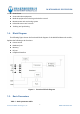
DX-BT24 MODULE SPECIFICATION Smart home Smart education equipment Medical equipment monitoring and wireless control Measurement and monitoring system Industrial sensors and controls Tracking and positioning 1.4. Block Diagram The following figure shows the functional block diagram of the DX-BT24 Bluetooth module, Explains the following main functions: Power section Baseband part Memory RF part Peripheral interface Figure 1:Functional block diagram 1.5.
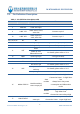
DX-BT24 MODULE SPECIFICATION Parameter Details Parameter Details Chip model DA14531 Module model DX-BT24 Bluetooth specifications BLE 5.1 Module size 26.6(L) x 12.8 (W) x 2.3(H) mm Operating Voltage 3.3V Working current 270 uA protocol GATT,ATT,GAP MTU value 253 bytes Sensitivity -94dBm@0.1%BER Transmit power -19.5~+2.5dBm Modulation GFSK Frequency band 2.402GHz -2.
DX-BT24 MODULE SPECIFICATION 2.2.
DX-BT24 MODULE SPECIFICATION 18,19,20,21 2.3.
DX-BT24 MODULE SPECIFICATION When connected: disconnected, the module automatically enters low power consumption mode; When it is not connected after waking up: You need to send the AT+PWRM command again to enter the low power consumption mode or reset, power off and restart to enter. For hardware, please refer to 2.5.5 wake-up circuit below. 2.4.2.
DX-BT24 MODULE SPECIFICATION Table 4:Power interface pin definition table Pin name Pin number describe Minimum Typical value VBAT 12 Module power 2.8 GND 13,14 Land - Max unit 3.3 3.6 V 0 - V 2.5.2. Power Supply Stability Requirements The power supply range of DX-BT24 is 2.8~3.6V. It is necessary to ensure that the input voltage is not lower than 2.8V. The following figure shows the voltage drop of VBAT during radio frequency burst transmission.
DX-BT24 MODULE SPECIFICATION 2.5.3. Power Down Requirements Since the working current of the chip of this module is very low, when the power is disconnected, if the IO port of the peripheral MCU has a weak current supplying the module, the module is likely to be in an abnormal working state at this time, so after disconnecting the power of the module, the MCU is connected to the module All IO ports must be configured as pull-down. 2.5.4.
DX-BT24 MODULE SPECIFICATION Figure 7:Key reset reference circuit 2.5.5.
DX-BT24 MODULE SPECIFICATION Pairing mode: After the slave module enters pairing mode, after the search mode of the master module is set to pairing mode, the master module will automatically connect to the slave module.This pairing mode is only valid for our main module. Figure 8:Open-collector drive wake-up reference circuit Figure 9:Key reset reference circuit 2.6. Hardware Physical Interface 2.6.1. UART Interface Shenzhen DX-SMART Technology Co., Ltd. - 15 - www.szdx-smart.
DX-BT24 MODULE SPECIFICATION Four signal pins are used to realize UART function. When DX-BT24 is connected to another digital device, UART_RX and UART_TX transfer data between the two devices. The remaining two pins, UART_CTS and UART_RTS, can be used to implement RS232 hardware flow control, and they are both active at low level, that is, transmission is allowed at low level, and transmission is stopped at high level.
DX-BT24 MODULE SPECIFICATION clock line (SCL). The I2C module provides two data transmission rates: 100kHz in standard mode and 400kHz in fast mode. The I2C module also has an arbitration detection function to prevent multiple hosts from attempting to transmit data to the l2C bus at the same time. Figure 10:IIC communication sequence diagram 2.6.4.
DX-BT24 MODULE SPECIFICATION 2.6.5. Analog-to-digital Converter(ADC) Typical 10-bit dynamic ADC of 125 ns Maximum sampling rate was 1 Msample/s Ultra-low power consumption (20 uA Typical power supply current, 100 ksample/s) Configurable attenuator: 1x, 2x,3x, 4x The device integrates a 10-bit high-speed and ultra-low-power general-purpose analog-to-digital converter (ADC). It can operate in unipolar (single-ended> mode and bipolar (differential) mode. ADC has its own 0.
DX-BT24 MODULE SPECIFICATION Figure 13:Reference circuit for serial port level conversion 3. Electrical Characteristics & Reliability 3.1. Maximum Rating The absolute maximum ratings of the supply voltage and voltage on the digital and analog pins of the module are listed below. Exceeding these values will cause permanent damage. The average GPIO pin output current is defined as the average current value flowing through any corresponding pin in a 100mS period.
DX-BT24 MODULE SPECIFICATION Table 10:Working voltage table Operating Voltage parameter Minimum Typical Max unit VIN- Core supply voltage(VDD) 2.8 3.3 3.6 V VIN- I/O power supply/voltage(VDDIO) 2.8 3.3 3.6 V 3.2. Working And Storage Temperature Table 11:Working and storage temperature table 3.3.
DX-BT24 MODULE SPECIFICATION 3.4. RF Characteristics Table 13:RF characteristics table Function 3.5. Value BLE transmit power -19.5 ~2.5dBm BLE sensitivity -94dBm@0.1%BER Static Protection In the application of the module, due to the static electricity generated by human body static electricity and charged friction between microelectronics, it is discharged to the module through various ways, which may cause certain damage to the module, so ESD protection should be taken seriously.
DX-BT24 MODULE SPECIFICATION 4.1. Module Mechanical Size Figure 14:Module top and side dimension drawing Figure 15:Bottom view size of the module Shenzhen DX-SMART Technology Co., Ltd. - 22 - www.szdx-smart.
DX-BT24 MODULE SPECIFICATION 4.2. Recommend Encapsulation Figure 16:Recommended package dimensions 4.3. Module Top View & Bottom View Figure 17:Top and bottom views of the module Remark The above picture is for reference only. For the actual product appearance and label information, please refer to the actual module. Shenzhen DX-SMART Technology Co., Ltd. - 23 - www.szdx-smart.
DX-BT24 MODULE SPECIFICATION 4.4. Hardware Design Layout Recommendations The DX-BT24 Bluetooth module works in the 2.4G wireless frequency band and uses an on-board antenna. The standing wave ratio (VSWR) and efficiency of the antenna depend on the placement of the patch. Various factors should be avoided as far as possible to the wireless signal transmission and reception. Pay attention to the following What time is it: 1、Avoid using metal for the product shell surrounding the Bluetooth.
DX-BT24 MODULE SPECIFICATION 5. 5.1. Patch Requirements Storage Conditions Modules are shipped in vacuum sealed bags. The humidity sensitivity level of the module is 3 (MSL 3), and its storage must comply with the following conditions: 1. Recommended storage conditions: temperature 23±5°C, and relative humidity 35~60%. 2. Under the recommended storage conditions, the module can be stored in a vacuum sealed bag for 12 months. 3.
DX-BT24 MODULE SPECIFICATION Remark 1. In order to prevent and reduce the occurrence of defective welding such as blistering and delamination caused by damp, strict control should be carried out. It is not recommended to expose to the air for a long time after unpacking the vacuum package. 2.
DX-BT24 MODULE SPECIFICATION Figure 19:Recommended reflow soldering temperature profile Table 15:Recommended reflow soldering temperature Statistics name Lower limit Upper limit Slope 1 (target=2.0) is between 30.0 and 70.0 unit 1 3 Degree/sec 1 3 Degree/sec -5 -0.5 Degree/sec Constant temperature time 110-190℃ 60 120 sec @220℃ Reflow time 30 65 sec Peak temperature 235 250 Celsius @235℃ total time 10 30 sec Slope 2 (target=2.0) is between 70.0 and 150.0 Slope 3 (target = -2.
DX-BT24 MODULE SPECIFICATION Figure 20:Carrier tape size(Unit: mm) Figure 21:Reel size (unit: mm) Shenzhen DX-SMART Technology Co., Ltd. - 28 - www.szdx-smart.
DX-BT24 MODULE SPECIFICATION Figure 22:Tape direction 6. 6.1. Certification CE-(Europe) Certificate NO:STS2101096RE 6.2. FCC-(U.S.A.) FCC IDENTIFIDR:2AKS8-DX-BT24 6.3. SRRC-(China) CMIIT ID:2021DP6828 Shenzhen DX-SMART Technology Co., Ltd. - 29 - www.szdx-smart.
FCC Statement This device complies with part 15 of the FCC Rules. Operation is subject to the following two conditions: (1) This device may not cause harmful interference, and (2) this device must accept any interference received, including interference that may cause undesired operation. Any Changes or modifications not expressly approved by the party responsible for compliance could void the user's authority to operate the equipment. The device has been evaluated to meet general RF exposure requirement.
Note: This equipment has been tested and found to comply with the limits for a Class B digital device, pursuant to part 15 of the FCC Rules. These limits are designed to provide reasonable protection against harmful interference in a residential installation. This equipment generates uses and can radiate radio frequency energy and, if not installed and used in accordance with the instructions, may cause harmful interference to radio communications.
Integration instructions for host product manufacturers according to KDB 996369 D03 OEM Manual v01 2.2 List of applicable FCC rules FCC Part 15 Subpart C 15.247 & 15.207 & 15.209 2.3 Specific operational use conditions The module is a Bluetooth module with BLE function. Operation Frequency: 2402-2480MHz Number of Channel: 40 Modulation: GFSK Type: PCB Antenna Gain: 0dBi The module can be used for mobile or portable applications with a maximum 0dBi antenna.
2.8 Label and compliance information Host product manufacturers need to provide a physical or e-label stating “Contains FCC ID: 2AKS8-DX-BT24 ” with their finished product. 2.