
Data Sheet
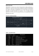

HRF24B21AN
©2021 Honeycomb Technologies Advance Information 10 page
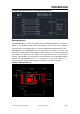
FIGURE 9 BOTTOM COPPER
FIGURE 10 PCB LAYER STACK UP
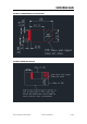
PCB Antenna
The PCB antenna is fabricated on the top copper trace. Figure 11 shows the trace
dimensions. The layers below the antenna have no copper traces. The ground and
power planes under the components serve as a counterpoise to the PCB antenna.
Additional ground plane on the host PCB will substantially enhance the performance
of the module.