
Service Manual


9
Circuit Description
Realization Methods for Basic Functional Modules
PLL Frequency Synthesizer
The PLL circuit generates local oscillator signals for reception and RF carrier signals for
transmission.
The PLL circuit consists of the VCO oscillator circuit and baseband processor chip and realizes
frequency tracking and channel conversion under the control of MCU signals.
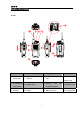
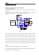
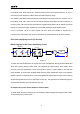
1. PLL
MB95F108AK
WPFV-GE1
U605
1/2
17bitDIV
32/33
OSC
1/2
21bitDIV
U202
CP
RX-VCO
L102
D103
L101
APC/TUNE
T/R-SW
CLK
DATA
EN
Q101
2SK508NV
D102
BUFFER
Q6
1
23
D104
D101
D100
Q100
2SK508NV
12.8MHZ
TX-VCO
LPF
Q5
1
23
Figure 2
The step frequency of the PLL circuit is 5.0KHz, 6.25KHz, 10.0KHz or 12.5KHz. Therefore, the
reference oscillator signal (38.4MHz) is divided into 5.0KHz, 6.25KHz, 10.0KHz or 12.5KHz
reference signals by a fixed counter in PLL of U202. Signals output by VCO pass through buffer
Q102 followed by amplifier Q103 and enters PLL of U200 for frequency division by a variable
divider. The signals from the frequency division are compared with reference signals in the phase
comparator PD of PLL. Signals output by the phase comparator is added to the varactors D100,
D101, D102 and D103 of VCO to control the output frequency after passing through a low pass
filter.
2. VCO
The VCO section is realized by the oscillator circuit of three-point capacitor.
In transmitting mode, the operation frequency of VCO is generated by Q100; in receiving mode, the
operation frequency of VCO is generated by Q101.