
Data Sheet
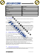
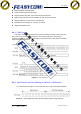


Table Of Contents

深圳市飞易通科技有限公司
www.feasycom.com
FSC-BT826
7.4 Drop test
Free fall the module (condition built in a wrapper which can defend ESD) from 150cm height to
cement ground, each side twice, total twelve times. The appearance will not be damaged and all
functions OK.
7.5 Packaging information
After unpacking, the module should be stored in environment as follows:
Temperature: 25℃ ± 2℃
Humidity: <60%
No acidity, sulfur or chlorine environment
The module must be used in four days after unpacking.
8. Layout and Soldering Considerations
8.1 Soldering Recommendations
FSC-BT826 is compatible with industrial standard reflow profile for Pb-free solders. The reflow
profile used is dependent on the thermal mass of the entire populated PCB, heat transfer efficiency of
the oven and particular type of solder paste used. Consult the datasheet of particular solder paste for
profile configurations.
Feasycom will give following recommendations for soldering the module to ensure reliable solder
joint and operation of the module after soldering. Since the profile used is process and layout
dependent, the optimum profile should be studied case by case. Thus following recommendation
should be taken as a starting point guide.
8.2
Layout Guidelines
It is strongly recommended to use good layout practices to ensure proper operation of the module.
Placing copper or any metal near antenna deteriorates its operation by having effect on the matching
properties. Metal shield around the antenna will prevent the radiation and thus metal case should not be
used with the module. Use grounding vias separated max 3 mm apart at the edge of grounding areas to
prevent RF penetrating inside the PCB and causing an unintentional resonator. Use GND vias all
around the PCB edges.
The mother board should have no bare conductors or vias in this restricted area, because it is not
covered by stop mask print. Also no copper (planes, traces or vias) are allowed in this area, because of
mismatching the on-board antenna.