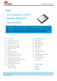
m1805 Module Specification Cost-sensitive m1805 Module MS48SF2 Specification UART module MS48SF2 is based on m1805 Chipset. It is a small size (16×12×2mm) and stand-alone module with 12 GPIO. The data transmission between module and mobile phone can be achieved via operation of UART. With up to 60-meter working distance in open space, 512KB flash memory, etc.
m1805 Module Specification Revision history Version Date Notes Contributor(s) Person of Approve V 1.0 2019.02.
m1805 Module Specification Index Revision history.......................................................................................................................................................................... 2 1. Product introduction.............................................................................................................................................................. 4 1.1 Ordering information.................................................................................
m1805 Module Specification 1. Product introduction UART module MS48SF2 is based on m1805 Chipset. It is a small size (16×12×2mm) and stand-alone module with 12 GPIO. The data transmission between module and mobile phone can be achieved via operation of UART. With up to 60-meter working distance in open space, 512KB flash memory and -97dBm received sensitivity, the data can be transmitted via Bluetooth. MS48SF2 is a compact module with a metal cover shield which can support Android 4.3+, IOS 7+.
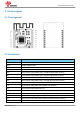
m1805 Module Specification 2. Pin description 2.1 Pin assignment 2.
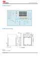
m1805 Module Specification 2.3 Block diagram 2.4 Mechanical drawing Unit: mm Tolerance: +/- 1.
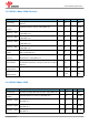
m1805 Module Specification 3. Electrical specification The electrical specifications of the module are directly related to the Specifications for the m1805 chipset. The below information is only the extract from m1805 specification. For more detailed information, please refer to the up-to-date specification of the chipset available. 3.1 Absolute maximum ratings Symbol Parameter Min. Max Unit -0.3 +3.6 V DEC 1.32 V VSS 0 V -0.3 VDD + 0.
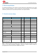
m1805 Module Specification 3.2 Recommended operating conditions Symbol Parameter Min. Nom. Max. Units VDD3 supply voltage,normal mode 1.8 3.0 3.6 V tr_VDD Supply rise time (0 V to 1.8 V) 100 ms TA Operating temperature 125 °C -40 27 Important : The On-chip power-on reset circuitry may not function properly for rise times longer than the specified maximum. 3.3 Electronic characteristic 3.3.1 General radio characteristics Parameter Description Min. TYP Max.
m1805 Module Specification 3.3.
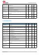
m1805 Module Specification Selectivity +-4MHz Wanted signal at -67dBm, modulated interferer at +/- 4MHz, 37 Byte BER=1E-3 Selectivity +-5MHz Wanted signal at -67dBm, modulated interferer at >=+/- 5MHz, or More 37 Byte BER=1E-3 Selectivity Imag frequency Wanted signal at -67dBm, modulated interferer at imagefrequency, 37 Byte BER=1E-3 40 I/C dB 55 I/C dB 22 I/C dB -20 dBm +-350 KHz +-120 ppm Wanted signal at 2402MHz, -64dBm, Two interferers at 2405 Intermodulation and 2408 MHz
m1805 Module Specification 3.3.
m1805 Module Specification 4.
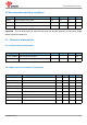
m1805 Module Specification 5. Package information 5.1 Package dimension Unit: mm Tolerance: +/- 0.
m1805 Module Specification Unit: mm Tolerance: +/- 0.1, default Details Reel Quantity(module) 850PCS Tape Weight 450g Single module Weight 0.6g Gross Weight 970g Dimension W:44mm T:0.
m1805 Module Specification 6. Reflow and soldering Profile Feature Sn-Pb Assembly Pb-Free Assembly Solder Paste Sn63/Pb37 Sn96.5/Ag3/Cu0.
m1805 Module Specification 7. Notes & cautions We cannot assure that the specification has no errors and omission even though this specification is under collate and check strictly. This specification is under the protection of laws and regulations of copyright, please do not copy and duplicate at any form, or do not transmit part or full of this specification in any wire and wireless network in any form, or do not edit or translate to any other format, word, code, etc. 7.
m1805 Module Specification The upper and below area of antenna (including the case) shall have 4mm or more than 4mm clearance to reduce the influences for antenna. *The Grey area above is Carrier board. 7.3 Installation and soldering (1) Please do not lay copper under the module antenna. It can prevent the influence of signal radiation and the transmission distance from being affected. 7.
m1805 Module Specification (2) Please store the modules within -40℃ to +125℃ before and after installation and make sure the modules is away from the direct sunlight exposure for a long duration. Modules should be far away from humid and salty air conditions, and any corrosive gasses or substances. (3) Please not to wash the module. No-Clean Paste is used in production. The metal shield may be oxidized by the washing process and may lead to chemistry reaction with No-Clean Paste.
m1805 Module Specification 9. Contact information Manufacturer: Shenzhen Minew Technologies Co., Ltd. Tel: 0086-755-2103 8160 Email: info@Minew.com URL: https://www.minew.
FCC WARNING This device complies with part 15 of the FCC Rules. Operation is subject to the following two conditions: (1) this device may not cause harmful interference, and (2) this device must accept any interference received, including interference that may cause undesired operation. Any changes or modifications not expressly approved by the party responsible for compliance could void the user's authority to operate the equipment.