
User's Manual


WM620 Hardware User Guide V1.1
All rights reserved by Shenzhen Neoway Technology Co., Ltd. Page 3
2 Applicable interface
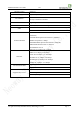
2.1 Power supply Interface
The Power supply part of the WM620 module contains:
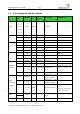
PIN
Signal name
I/O
Function description
Note
22、23
VBAT
PWR
For power voltage input
47
VRTC
PWR
Coin cell backup voltage input
26
VDD_1.8V
PWR
Linear regulator 1.8V output
27
VDD_2.6V
PWR
Linear regulator 2.6V output
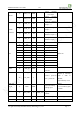
Characteristics of the VBAT are shown in the table 2-1.
Table 2-1, Input voltage characteristics
Status
Min. voltage
Typical voltage
Max. voltage
VBAT
+3.3 VDC
+3.8 VDC
+4.2VDC
NOTE:Make sure that the VBAT can never exceed 4.5VDC. Voltage higher than 4.5VDC may damage the
WM620 module.
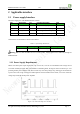
2.1.1 Power Supply Requirements
VBAT is the main power input ranged from 3.3V to 4.2V DC, 3.8V DC is recommended. The average current
is less than 500mA@3.8VDC. But in the module’s transmitting mode, the largest current can burst up to 1.8A
providing the RF power amplifier. The burst current may cause deep voltage drop, and trigger the module into
a power reset. Thus a high value and low ESR capacitor must be installed on the VBAT, to avoid or reduce the
voltage drop caused by the RF power amplifier.
Figure 2-1a, current and voltage curve of VBAT