
User's Manual


N
720 Hardware User Guide
Copyright © Neoway Technology Co., Ltd iii
Contents
1 Introduction to N720 ........................................................................................................ 1
1.1 Overview ........................................................................................................................................... 1
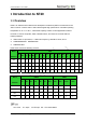
1.2 Block Diagram .................................................................................................................................. 2
1.3 Features ............................................................................................................................................ 2
2 Application Interfaces ..................................................................................................... 5
2.1 Specifications and Pin Definition ................................................................................................... 5
2.2 Pin Description ................................................................................................................................. 6
2.3 Power Control Interfaces .............................................................................................................. 13
2.3.1 VBAT ...................................................................................................................................... 13
2.3.2 VDDIO_1P8 ........................................................................................................................... 17
2.3.3 ON/OFF ................................................................................................................................. 17
2.3.4 RESET ................................................................................................................................... 19
2.4 USB Interface ................................................................................................................................. 21
2.5 UIM Card Interface ........................................................................................................................ 22
2.6 GPIO ................................................................................................................................................ 24
1.1.1 UART ...................................................................................................................................... 24
2.6.2 ADC ........................................................................................................................................ 26
2.6.3 NET_LIGHT ........................................................................................................................... 26
2.6.4 DTR ........................................................................................................................................ 27
2.6.5 RING Signal Indicator .......................................................................................................... 27
2.7 Commissioning Interfaces ............................................................................................................ 28
2.7.1 FORCE_USB_BOOT ........................................................................................................... 28
3 RF Interface ...................................................................................................................... 29
3.1 2G/3G/4G RF Design and PCB Layout ...................................................................................... 29
3.2 GPS RF Design and PCB Layout ............................................................................................... 31
3.2.1 GPS Impedance ................................................................................................................... 31
3.2.2 Active GPS Antenna Design ............................................................................................... 31
4 Electric Feature and Reliability ................................................................................... 33
4.1 Electric Feature .............................................................................................................................. 33
4.2 Temperature.................................................................................................................................... 33
4.3 ESD Protection ............................................................................................................................... 34
5 RF Feature ........................................................................................................................ 35
5.1 Work Band ...................................................................................................................................... 35