RF-BM-4044B2 Bluetooth Low Energy Module Version 1.1 Shenzhen RF-star Technology Co., Ltd. Aug.
RF-BM-4044B2 www.szrfstar.com Ver1.1 - Aug., 2018 1 Device Overview 1.1 Description RF-BM-4044B2 module is designed based on CC2640R2FRSM Bluetooth Smart BT 5.0 System-on-Chip, fully supports the single mode Bluetooth Low Energy operation. The module contains a 32-bit ARM CortexTM-M3 processor, with the working frequency at 48.0 MHz which is the same as the main processor.
RF-BM-4044B2 www.szrfstar.com Ver1.1 - Aug., 2018 • Smart door locks • Energy harvesting • Phone accessories • Thermometer • Health-care equipment • Human input devices • Smart lighting • Sports equipment Shenzhen RF-star Technology Co., Ltd.
RF-BM-4044B2 www.szrfstar.com Ver1.1 - Aug., 2018 Table of Contents 1 Device Overview ............................................................................................................................................................ 1 1.1 Description .......................................................................................................................................................... 1 1.2 Key Features ..........................................................................
RF-BM-4044B2 www.szrfstar.com Ver1.1 - Aug., 2018 Table of Figures Figure 1. Functional Block Diagram of RF-BM-4044B2 ........................................................................................... 2 Figure 2. The Pin Diagram of RF-BM-4044B2 ......................................................................................................... 6 Figure 3. The Photos of RF-BM-4044B2 ...............................................................................................................
RF-BM-4044B2 www.szrfstar.com Ver1.1 - Aug., 2018 2 Module Configuration and Functions 2.1 Module Parameters Table 1. The Parameters of RF-BM-4044B2 Chipset CC2640R2FRSM Supply Power Voltage 1.8 V ~ 3.8 V, recommended to 3.3 V Frequency 2402 MHz ~ 2480 MHz Maximum Transmit Power -21.0 dBm ~ +2.5 dBm Receiving Sensitivity -97 dBm GPIO 10 Crystal 24 MHz RAM 20 KB Flash 128 KB Package SMT Packaging Frequency Error ±20 kHz Dimension 16.6 mm x 11.2 mm x 1.
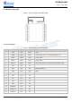
RF-BM-4044B2 www.szrfstar.com Ver1.1 - Aug., 2018 2.2 Module Pin Diagram Figure 2. The Pin Diagram of RF-BM-4044B2 3.3 Pin Functions Table 2. The Pin Diagram of RF-BM-4044B2 Pin Name Chip Pin Pin Type 1 GND GND Power GND 2 VDDZ VCC Power Power supply 1.8 V ~ 3.8 V, Recommend 3.3 V 3 TMSC TMSC JTAG JTAG: TMSC 4 TCKC TCKC JTAG JTAG: TCKC 5 RES_N REST REST Reset after power on. No need for external RC circuit.
RF-BM-4044B2 www.szrfstar.com Ver1.1 - Aug., 2018 17 P00/RX P0.0 I/O 18 NC - - 3 Specifications 3.1 Recommended Operating Conditions Functional operation does not guarantee performance beyond the limits of the conditional parameter values in the table below. Long-term work beyond this limit will affect the reliability of the module more or less. Table 3. Recommended Operating Conditions of RF-BM-4044B2 Items Condition Min. Typ. Max. Unit Operating Supply Voltage Battery Mode 1.8 3.3 3.
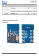
RF-BM-4044B2 www.szrfstar.com Ver1.1 - Aug., 2018 Test Item Parameter Test Value Unit 5 (Max.) dBm Frequency Error ±20 KHz Radiation (30 m ~ 1 G) -36 dBm Radiation (1 G ~ 12.75 G) -30 dBm Sensitivity (8% PER) -93 dBm Power Transmitter Receiver 4 Application, Implementation, and Layout 4.1 Module Photos Figure 3. The Photos of RF-BM-4044B2 Shenzhen RF-star Technology Co., Ltd.
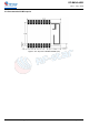
RF-BM-4044B2 www.szrfstar.com Ver1.1 - Aug., 2018 4.2 Recommended PCB Footprint Figure 4. The Top View of RF-BM-4044B2 (mm) Shenzhen RF-star Technology Co., Ltd.
RF-BM-4044B2 www.szrfstar.com Ver1.1 - Aug., 2018 4.4 Basic Operation of Hardware Design 1. It is recommended to offer the module with a DC stabilized power supply, a tiny power supply ripple coefficient and the reliable ground. Please pay attention to the correct connection between the positive and negative poles of the power supply. Otherwise, the reverse connection may cause permanent damage to the module; 2. Please ensure the supply voltage is between the recommended values.
RF-BM-4044B2 www.szrfstar.com Ver1.1 - Aug., 2018 Layer, the copper must be spread on the connection part of the top layer and the module, and be close to the digital part of module and routed in the Bottom Layer (all copper is well grounded). 5. Assuming that the module is soldered or placed in the Top Layer, it is also wrong to randomly route the Bottom Layer or other layers, which will affect the spurs and receiving sensitivity of the module to some degrees; 6.
RF-BM-4044B2 www.szrfstar.com Ver1.1 - Aug., 2018 voltage. 2. Please ensure the anti-static installation and the electrostatic sensitivity of high-frequency devices. 3. Due to some humidity sensitive components, please ensure the suitable humidity during installation and application. If there is no special demand, it is not recommended to use at too high or too low temperature. 4.5.3 High Bit Error Rate 1. There are co-channel signal interferences nearby.
RF-BM-4044B2 www.szrfstar.com Ver1.1 - Aug., 2018 5 Certification 5.1 FCC warnings FCC Statement FCC standards: FCC CFR Title 47 Part 15 Subpart C Section 15.247 Integral PCB antenna with antenna gain 0dBi This device complies with part 15 of the FCC Rules. Operation is subject to the following two conditions: (1) This device may not cause harmful interference, and (2) this device must accept any interference received, including interference that may cause undesired operation.