
- enhanced real-time ethernet controller User Manual
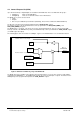

2.10 ARM946E-S Register
The ARM946E-S uses CP15 registers for system control.
Consequently, the following settings are possible:
• Configure cache type and cache memory area
• Configure tightly coupled memory area
• Configure memory protection unit for various regions and memory types
• Assign system option parameters
• Configure “Little Endian” or “Big Endian” operations
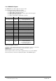
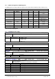
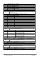
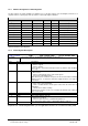
Register Access Description
0 R
ID code register (1)
Cache type register (1)
Tightly coupled memory size register (2)
1 W/R Control register
2 W/R Cache configuration register (2)
3 W/R Write buffer control register
4 xxx
Undefined
5 W/R Access permission register (2)
6 W/R Protection region base/size register (2)
7 W Cache operation register
8 xxx
Undefined
9 W/R Cache lockdown register (2)
10 xxx
Undefined
11 xxx
Undefined
12 xxx
Undefined
13 W/R Trace process ID register
14 xxx
Undefined
15 W/R
RAM/TAG-BIST test register (1)
Test state register (1)
Cache debug index register (1)
Trace control register
Table 5: CP15 Registers - Overview
(1) Registers contain multiple information entries that are selected by the “opcode_2” or “CRm” fields.
(2) Separate registers for instruction and data (see detailed description of registers).
Undefined means:
When this register is read, the read value is undefined.
When this register is written to, unforeseeable configuration changes can occur in the ARM946.
Refer to documents /1/ and /2/ for a detailed description of the ARM946 registers.
Copyright © Siemens AG 2007. All rights reserved. 31 ERTEC 200 Manual
Technical data subject to change Version 1.1.0