ERTEC 200 Enhanced Real-Time Ethernet Controller PHY Description Copyright © Siemens AG 2008. All rights reserved. Technical data subject to change Page 1 ERTEC 200 PHY Version 1.0.
Edition (11/2007) Disclaimer of Liability We have checked the contents of this manual for agreement with the hardware and software described. Since deviations cannot be precluded entirely, we cannot guarantee full agreement. However, the data in this manual are reviewed regularly. Necessary corrections are included in subsequent editions. Suggestions for improvement are welcomed. Copyright © Siemens AG 2007.
This manual will be updated as required. You can find the current version of the manual on the Internet at http://www.siemens.com/comdec. Guide To help you quickly find the information you need, this manual contains the following aids: o A complete table of contents as well as a list of all figures and tables in the manual are provided at the beginning of the manual. o A glossary containing definitions of important terms used in the manual is located following the appendices.
Contents Multiport Ethernet PHY’s for ERTEC200 ........................................................................................6 1.1 Introduction ............................................................................................................................................ 6 1.2 PHY Interface Pin Functions .................................................................................................................. 7 1.3 Functional Description........................................
List of Figures Figure 1: PHY Block Diagram ................................................................................................................................8 Figure 2: MLT-3 Encoding Example....................................................................................................................12 Figure 3: Internal and Remote Loopback Modes...............................................................................................17 Figure 4: Phase Offset Indicator Function ...
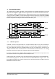
Multiport Ethernet PHY’s for ERTEC200 1.1 Introduction ERTEC 200 has integrated a 2 channel multiport Ethernet PHY (Physical Layer Transceiver), that supports the following transmission modes: • 10BASE-T • 100BASE-TX • 100BASE-FX It can be connected to unshielded twisted-pair (UTP) cable via external magnetics or to optical fiber via fiber PMD modules. Internally on the ERTEC 200 it interfaces to the MAC layer through the IEEE 802.3 Standard Media Independent Interface (MII).
1.
1.3 Functional Description This chapter gives a functional description of the integrated PHYs on ERTEC 200 based on the block diagram shown in Figure 1 . Figure 1 shows a single channel; both channels have identical structure. The subsequent chapters will frequently refer to signals that are present on the MII interface between on-chip PHY and on-chip MAC. In these cases the signal names that have been introduced in \1\Table 1.5.7 and 1.5.8 will be used.
The PHY realizes a complete 10BASE-T transceiver function. It includes the receiver, transmitter and the following functions. <1> <2> <3> <4> <5> <6> Filter and squelch Jabber detection Signal quality error (SQE) message test function Timing recovery from received data Manchester encoding/decoding Full-duplex or Half-duplex mode In half-duplex mode, the PHY transmits and simultaneously receives in order to provide loopback of the transmitted signal. (Refer to section 14.2.1.3 of IEEE802.
1.3.2 100BASE-TX Operation 100BASE-TX specifies operation over two copper media: two pairs of shielded twisted-pair cable (STP) and two pairs of unshielded twisted-pair cable (Category 5 UTP). 100BASE-TX function includes the physical coding sub-layer (PCS), the physical medium attachment (PMA) and physical medium dependent sub-layer (PMD). When transmitting, 4-bit data nibbles come from the MII interface at a rate of 25 MHz and are converted to 5-bit encoded data.
(4) 4B/5B encoding/decoding In 100BASE-TX mode, 4B/5B coding is used. The 4B/5B encoder converts 4-bit nibbles coming from the MII interface to 5-bit symbols that are referred to as “code-groups”. The relation between original and encoded data is shown in Table 2. For testing purposes the encoder and decoder can be bypassed with the Enable 4B5B bit in the PHY special control/status register.
(5) Scrambling/Descrambling Scrambling the data before transmission helps to eliminate large narrow-band signal power peaks for repeated data patterns, and spreads the signal power more uniformly over the entire channel bandwidth. The scrambler encodes a plaintext NRZ bit stream by addition (modulo 2) of 2047 bits generated by the recursive linear function X[n]= X[n-11] + X[n-9] (modulo 2).
(7) Receive Data Valid / Receive Error The receive data valid signal RX_DV_P(2:1) indicates that recovered and decoded nibbles are being presented on the RXD_P1(3:0) respectively RXD_P2(3:0) outputs synchronous to RX_CLK_P(2:1). RX_DV_P(2:1) becomes active after the /J/K/ delimiter has been recognized and RXD_P(2:1) is aligned to nibble boundaries. It remains active until either the /T/R/ delimiter is recognized or link test indicates failure.
FEFI consists of a modification to the IDLE code patterns. In this mode, every 16 IDLE code groups are followed by a data-0 code group. If the PHY detects a FEFI pattern in its receive stream, it deasserts its link status and transmits only IDLE patterns (not FEFI) on its transmit stream. A full description of the Far End Fault Function is given in Section 24.3.2.1 in the IEEE 802.3 standard. 1.3.
(3) Priority Resolution If two Ethernet communication partners negotiate their capabilities, there are four possible matches of the technology abilities. In the order of priority these are: • 100M full Duplex (highest priority) • 100M Half Duplex • 10M full Duplex • 10M Half Duplex (lowest priority) Since two devices (local device and remote device) may have multiple abilities in common, a prioritization scheme exists to ensure that the highest common denominator ability is chosen.
1.3.5 Miscellaneous Functions This chapter summarizes some additional functions of the PHYs. (1) LED indicators Six LED signals are provided per PHY. These provide a convenient means to determine the operation mode of the PHYs. All LED signals are active low. The LED signals are made available through the GPIO pins of the ERTEC 200.
(2) MDI/MDI-X crossover detection The PHYs automatically detect and correct MDI/MDI-X crossover. This function can be disabled by setting the AutoMDIX_en bit in the Mode Control/Status register to 0b. When it is disabled, crossover must be corrected manually by setting the MDI mode bit in the same register accordingly. (3) Polarity This core automatically detects and corrects polarity reversal in wiring in 10BASE-T mode.
In this mode, the complete preamble, SFD and EFD are re-generated by the PHY so that always complete packets are transmitted, even if received packets lack part of the preamble. The Isolate bit in the Basic Control register needs to be cleared to work in remote loopback mode. (5) Power Down Modes (a) Hardware power down This state is entered after a hardware reset of ERTEC 200. The PHYs are switched off and their power consumption is almost 0 W.
If the PowerOn reset is used, the PHYs are active after reset; if RES_PHY_N is used, the PHYs remain in power down mode after reset and must subsequently be activated with the PowerDown bit in the Basic Control register. The HW reset must be present for at least 100 µs. These reset signals are internally extended by 5.2 ms to ensure that the PHY is properly reset. All analog circuits and all digital logic including management registers are initialized.
(8) Interrupt handling Each PHY can generate a collective interrupt that can be triggered by several PHY-internal events; these two interrupts are routed with a wired-OR to the common IRQ9 input of the ERTEC 200 interrupt controller.
(11) Link Lockup Protection During the reception of 10BASE-T data, the link partner may switch to 100BASE-TX without starting auto-negotiation. In this case, the PHY must recognize this, de-assert the link status, and switch to 100BASE-TX mode. To achieve this, a counter is activated at the beginning of every 10BASE-T packet.
1.4 PHY Related Interfaces Like any other peripheral on the ERTEC 200 the PHYs have internal registers that allow control over their behaviour and that reflect their operation status; however in contrast to the other peripherals, the PHY control registrs are not memory mapped and not directly accessible for the ARM CPU core or any other AHB master within ERTEC 200. This is due to the standardized MII/SMI interface between the PHYs and the MACs that are integrated in the IRT switch.
PHY Pin NameNote Function TXD_P2(3:0) O Transmit data port 2 bits LBU_D(9:6) RXD_P23 O Receive data port 2 bit 3 LBU_A11/PIPESTA2 RXD_P22 O Receive data port 2 bit 2 LBU_A10/TRACESYNC RXD_P21 O Receive data port 2 bit 1 LBU_A9/TRACEPKT0 RXD_P20 O Receive data port 2 bit 0 LBU_A8/TRACEPKT1 TX_EN_P2 O Transmit enable port 2 LBU_D10 PHY 2 CRS_P2 PHY1 Alternate FunctionNote I/O O Carrier sense port 2 LBU_A12 RX_ER_P2 O Receive error port 2 PIPESTA0 TX_ERR_P2 O Transmit er
Note: SMI diagnosis interface pins are alternatively used as local bus interface or trace pins; in this table the I/O type is listed for the SMI diagnosis function (3) MDI Interface The media dependent interface (MDI) is the PHY’s data communication interface to the Ethernet network in 10BASE-T, 100BASE-TX or 100BAE-FX mode. It is partly analog and partly digital; the circuitry that is connected to the MDI interfaces must be carefully selected. Proposals can be found in Chapter 1.6.
Table 3 shows the assignment of GPIO pins to these status informations. (6) Other Signals There are a few other signals - mainly supply voltages - related to the PHYs summarized in Table 8. Pin NameNote RES_PHY_N EXTRES I/O Alternate FunctionNote Function O Reset signal to PHYs I/O External reference resistor (12.4 kΩ) LBU_D14 Note - DVDD(4:1) I Digital power supply, 1.
During a hardware reset or when the PHYs are driven out of the power down state (by setting the P1/2_PHY_ENB bits in the PHY_CONFIG register to 1b), a pre-defined configuration is set in the registers. This configuration is partly hardwired and affects the initial settings of PHY-internal registers. Table 10 shows these settings; the initial configuration can be altered later by writing to the PHY-internal registers.
Bit position Bit name 15 Reset R/W Function R/W Reset Resets the complete PHY Reset Software reset 0b Normal operation (initial value) 1b Execute a software reset for the affected PHY Note: This bit is self-clearing; it is automatically set to 0b by the reset pro cess.
Bit position Bit name 10 Isolate Function R/W R/W Isolate Isolates the PHY electrically from MII interface. Isolate Isolate mode control 0b Normal operation (initial value after device reset) 1b Puts PHY into isolate mode Note: The initial value, after only the PHY has been reset, is selected by the contents of the Pn_PHY_MODE field in the PHY_CONFIG register. 9 Restart Auto- R/W Restart Auto-Negotiation Restarts the auto-negotiation process.
1.5.2 Basic Status Register 15 14 13 12 11 -T4 7 10 9 8 Reserved 10Mb/s 100BASE 100BASE 100BASE 10Mb/s -TX Full -TX Half Full Half Duplex Duplex Duplex Duplex 6 5 4 3 2 1 Auto- Remote Auto- Link Sta Jabber Extended Negotiatio Fault Negotiatio tus Detect Capability Reserved N0.
Bit position Bit name R/W 11 10Mb/s Half R Duplex Function 10Mb/s Half Duplex Indicates ability to support 10Mb/s half duplex mode 10Mb/s Half Duplex 10Mb/s half duplex ability indication 0b 10Mb/s half duplex ability 1b 10Mb/s half duplex supported (initial value) 10:6 - R Reserved 5 Auto- R Auto-Negotiation Complete Negotiation Indicates, if auto-negotiation process has been completed Complete Auto-Negotiation Auto-negotiation completion indication Complete 0b Auto-negotiation ha
Bit position Bit name R/W 1 Jabber R Function Jabber Detect Detect Indicates, if a jabber condition has been detected Jabber Detect Jabber condition detection indication 0b No jabber condition has been detected (initial value) 1b Jabber condition has been detected Note: This bit is cleared, when it has been read.
The setting shown in Table 16 is the initial value, after the PHYs have been reset. As both registers as writable, the PHY ID number can be changed arbitrarily. 1.5.3 PHY Identifier Register REG2OUIIN 15 14 13 12 11 10 9 8 PHY ID Number 7 6 5 4 3 2 1 No.
1.5.5 Auto Negotiation Advertisment Register 15 14 13 12 11 Next Reserved Remote Reserved Page Fault 10 Pause Operation 9 8 100BASE 100BASE -T4 No. Initial value 4 xxxxHNote -TX Full duplex 7 6 5 4 3 100BASE 10BASE- 10BASE-TX T Full 2 1 0 Selector Field T Duplex Table 21: Auto-Negotiation Advertisement Register Overview Note: The initial value depends on the setting of the P(2:1)_PHY_MODE(2:0) bits in the PHY1/2 Configuration Register in the System Control Register block.
Bit position Bit name R/W 9 100BASE-T4 R Function 100BASE-T4 Indicates, if 100BASE-T4 operation is supported 100BASE-T4 0b 100BASE-T4 operation support indication No 100BASE-T4 operation support (initial value after device reset) 1b 100BASE-T4 operation support Note: The initial value, after only the PHY has been reset, is selected by the contents of the Pn_PHY_MODE field in the PHY_CONFIG register.
Bit position Bit name 5 10BASE-T R/W Function R/W 10BASE-T Indicates, if 10BASE-T operation mode is supported 10BASE-T 10BASE-T operation support 0b No 10BASE-T operation support (initial value after device reset) 1b 10BASE-T operation support Note: The initial value, after only the PHY has been reset, is selected by the contents of the Pn_PHY_MODE field in the PHY_CONFIG register. 4:0 Selector R/W Selector Field Field Indicates basic capabilities according to the IEEE802.
Bit position Bit name R/W 15 Next Page R Function Next Page Indicates if additional next page with link information will follow.
Bit position Bit name R/W 8 100BASE- R Function 100BASE-TX Full Duplex TX Full Indicates, if 100BASE-TX full duplex operation is supported by the link Duplex partner 100BASE-TX Full 100BASE-TX full duplex operation support Duplex 0b 100BASE-TX full duplex operation not supported by the link partner (initial value) 1b 100BASE-TX full duplex operation supported by the link partner 7 100BASE- R TX 100BASE-TX Indicates, if 100BASE-TX operation is supported by the link partner 100BASE-TX 100
1.5.7 Auto Negotiation Link Partner Ability Register – Next Page 15 Next 14 13 12 11 Acknowle Message Acknowle Page dge Page dge 2 7 6 5 4 10 Toggle 9 8 No. Initial value 5 0000H Message/Unformatted Code field 3 2 1 0 Message/Unformatted Code field Table 25: Auto-Negotiation Link Partner Ability Register Overview – Next Page Bit position Bit name R/W 15 Next Page R Function Next Page Indicates if additional next page with link information will follow.
1.5.8 Auto Negotiation Expansion Register 15 14 13 12 11 10 9 8 No.
Bit position Bit name 0 Link Partner Auto- R/W Function R Link Partner Auto-Negotiation Able Indicates if the link partner is auto-negotiation able or not Negotiation Able Link Partner Auto- Link partner auto-negotiation ability indication Negotiation Able 0b Link partner is not auto-negotiation able (initial value) 1b Link partner is auto-negotiation able Table 28: Auto-Negotiation Expansion Register Description Copyright © Siemens AG 2008. All rights reserved.
1.5.9 Auto Negotiation Next Page Transmit Register 15 14 13 12 11 Next Reserved Message Acknowle Page Page dge 2 5 4 7 6 10 Toggle 9 8 No. Initial value 7 2001H Message/Unformatted Code field 3 2 1 0 Message/Unformatted Code field Table 29: Auto-Negotiation Next Page Transmit Register Overview Bit position Bit name 15 Next Page R/W Function R/W Next Page Indicates if next page with link information exists.
1.5.10 Silicon Revision Register 15 14 13 12 11 10 Reserved 7 6 5 4 9 8 No.
1.5.11 Mode Control/Status Register 15 14 13 Reserved 12 11 10 9 8 No.
Bit position Bit name 7 AutoMDIX_ R/W Function R/W AutoMDIX_en en Enables the state machine for automatic detection of MDI/MDIX mode AutoMDIX_en 0b Automatic MDI/MDIX detection enable State machine for automatic MDI/MDIX detection disabled (initial value after device reset) 1b State machine for automatic MDI/MDIX detection enabled Note: The initial value, after only the PHY has been reset, is selected by the contents of the Pn_AUTOMDIXEN bit in the PHY_CONFIG register.
1.5.12 Special Mode Register 15 14 13 MIIMODE 12 11 Reserved 10 9 FX_MOD 8 Reserved No. Initial value 18 000xH E 7 6 5 4 3 PHY_MODE 2 1 0 PHY_ADD Table 35: Special Mode Register Overview Bit position Bit name R/W 15:13 MIIMODE R/W MIIMODE Function Selects different interface types between PHY and MAC.
Bit position 7:5 Bit name R/W Function PHY_MODE R/W PHY_MODE Selects between different operation modes of the PHYs.
1.5.13 Special Conrol/Status Indication Register 15 14 13 Reserved 12 11 10 9 SWRST_ SQEOFF 8 Reserved No.
1.5.14 Interrupt Source Flag Register 15 14 13 12 11 10 9 8 No.
Bit position Bit name R/W 3 INT3 R Function INT3 Indicates, if a link partner acknowledge has been received during the autonegotiation process INT3 Link partner acknowledge interrupt 0b No link partner acknowledge interrupt has been generated (initial value) 1b Link partner acknowledge interrupt has been generated 2 INT2 R INT2 Indicates, if a parallel detection fault has occurred INT2 Parallel detection fault interrupt 0b No parallel detection fault interrupt has been gen erated (initial
1.5.15 Interrupt Mask Register 15 14 13 12 11 10 9 8 Reserved 7 6 5 4 3 2 1 Mask bits No. Initial value 30 0000H 0 Reserved Table 41: Interrupt Mask Register Overview Bit position Bit name R/W 15:8 - R 7:1 Mask bits Function Reserved Write 0b; ignore on read access R/W Mask bits Mask each interrupt from interrupt flag register separately Mask bit n (n=1,..., 7) 0b Interrupt n masking (n=1,...
Bit position Bit name 15:13 - R/W Function R/W Reserved Write 000b; ignore on read access 12 Autodone R Autodone Indicates, if auto-negotiation is done Autodone Auto-negotiation done indication 0b Auto-negotiation is not done or is disabled (initial value) 1b 11:7 - Auto-negotiation is done R/W Reserved Write 00H; ignore on read access 6 Enable 4B5B R/W Enable 4B5B Allows to bypass the 4B/5B encoder/decoder.
1.6 Board Design Recommendations In this chapter some board design recommendations will be given with respect to • supply voltage circuitry • “line” interfaces for 10BASE-T, 100BASE-TX and 100BASE-FX • unused “line” interfaces 1.6.1 Supply Voltage Circuitry ERTEC 200 works with two operating voltages: VDD Core (1.5 V) and VDD IO (3.3 V). Additionally the on-chip PLL for the device clock generation requires a supply voltage called PLL_AVDD of 1.5 V, that is typically a filtered version of VDD Core.
GN VDD Core VDD IO (3.3 Power Decoupling with 0.1µF Decoupling with 10nF and 22nF as close to DVDD DGND DVDD DGND P2VDDARXT P2VSSAR P2VSSATX P2VSSATX VSSAPLLC VDDAC VDDAPL P1VSSATX P1VSSATX P1VSSAR P1VDDARXT GND33ES VDD33ES DGND DVDD DVDD DGND ERTEC Figure 6: Decoupling Capacitor Usage 1.6.2 10BASE-T and 100BASE-TX Mode Circuitry The analog input and output signals are very noise sensitive and PCB layout of these signals should be done very carefully.
3.3 V 10 Ω • 50 Ω 50 Ω • Unmarked resistors: 1/16 W and 1% tolerance Resistors marked with „•“: 1/8 W and 1% tolerance P(2:1)TxP 1 P(2:1)TxN 2 4 10 nF 75 Ω 75 Ω 5 AGND See Table 46 10 Ω • 50 Ω • 50 Ω ERTEC 200 RJ45 P(2:1)RxN 3 P(2:1)TxP EXTRES 6 7 10 nF 12.4k 75 Ω AGND 75 Ω 8 10 nF / 2 kV Case GND Figure 8: 10BASE-T and 100BASE-TX Interface Circuit Example 2 Table 46 shows some alternatives for the magnetics used in the previous circuits.
P(2:1)TDxP open P(2:1)TDxN open P(2:1)RDxN ERTEC P(2:1)RDxP P(2:1)SDxN P(2:1)SDxP GND (PECL) Figure 9: Circuit for Unused 100BASE-FX Mode Copyright © Siemens AG 2008. All rights reserved. Technical data subject to change Page 55 ERTEC 200 PHY Version 1.0.
1.6.3 100BASE-FX Circuitry In case of 100BASE-FX operation a standard optical transceiver module (like Agilent HFBR-5803) is connected to the P(2:1)RDxN, P(2:1)RDxP, P(2:1)SDxN, P(2:1)SDxP, P(2:1)TDxN and P(2:1)TDxP pins. The connection is straight forward and consists mainly of pull-up and pull-down resistors. The signals between the PHYs and the transceiver module(s) are 100 Ω differential respectively 50 Ω single-ended signals. This must be taken into account during PCB design.
2 2.1 /1/ Miscellaneous References: ERTEC 200 Manual V1.1.0 (ERTEC200_Manual_V110.