
User`s manual

Memory Organization
C515
Semiconductor Group 3-4
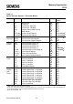
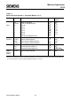
Table 3-1
Special Function Registers - Functional Blocks
Block Symbol Name Address Contents after
Reset
CPU ACC
B
DPH
DPL
PSW
SP
SYSCON
SYSCON
4)
Accumulator
B-Register
Data Pointer, High Byte
Data Pointer, Low Byte
Program Status Word Register
Stack Pointer
System Control Register
System Control Register
E0
H
1)
F0
H
1)
83
H
82
H
D0
H
1)
81
H
B1
H
B1
H
00
H
00
H
00
H
00
H
00
H
07
H
XX1X XXXX
B
3)
XXXX XXXX
B
3)
A/D-
Converter
ADCON
2)
ADDAT
DAPR
A/D Converter Control Register
A/D Converter Data Register
A/D Converter Program Register
D8
H
1)
D9
H
DA
H
00X0 0000
B
3)
00
H
00
H
Interrupt
System
IEN0
2)
IEN1
2)
P0
2)
IP1
IRCON
TCON
2)
T2CON
2)
SCON
2)
Interrupt Enable Register 0
Interrupt Enable Register 1
Interrupt Priority Register 0
Interrupt Priority Register 1
Interrupt Request Control Register
Timer Control Register
Timer 2 Control Register
Serial Channel Control Register
A8
H
1)
B8
H
1)
A9
H
B9
H
C0
H
1)
88
H
1)
C8
H
1)
98
H
1)
00
H
00
H
00
H
X000 0000
B
3)
XX00 0000
B
3)
00
H
00
H
00
H
Timer 0/
Timer 1
TCON
2)
TH0
TH1
TL0
TL1
TMOD
Timer 0/1 Control Register
Timer 0, High Byte
Timer 1, High Byte
Timer 0, Low Byte
Timer 1, Low Byte
Timer Mode Register
88
H
1)
8C
H
8D
H
8A
H
8B
H
89
H
00
H
00
H
00
H
00
H
00
H
00
H
Compare/
Capture
Unit /
Timer 2
CCEN
CCH1
CCH2
CCH3
CCL1
CCL2
CCL3
CRCH
CRCL
TH2
Comp./Capture Enable Reg.
Comp./Capture Reg. 1, High Byte
Comp./Capture Reg. 2, High Byte
Comp./Capture Reg. 3, High Byte
Comp./Capture Reg. 1, Low Byte
Comp./Capture Reg. 2, Low Byte
Comp./Capture Reg. 3, Low Byte
Com./Rel./Capt. Reg. High Byte
Com./Rel./Capt. Reg. Low Byte
Timer 2, High Byte
C1
H
C3
H
C5
H
C7
H
C2
H
C4
H
C6
H
CB
H
CA
H
CD
H
00
H
00
H
00
H
00
H
00
H
00
H
00
H
00
H
00
H
00
H
1) Bit-addressable special function registers
2) This special function register is listed repeatedly since some bits of it also belong to other functional blocks.
3) “X“ means that the value is undefined and the location is reserved
4) For C515-LN/1RN only