
User`s manual


Semiconductor Group 5-5
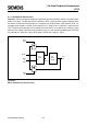
Reset / System Clock
C515
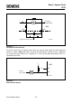
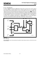
Figure 5-4
On-Chip Oscillator Circuitry
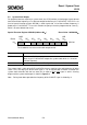
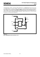
To drive the C515 with an external clock source, the external clock signal has to be applied to
XTAL2, as shown in figure 5-5. XTAL1 has to be left unconnected. A pullup resistor is suggested
(to increase the noise margin), but is optional if V
OH
of the driving gate corresponds to the V
IH2
specification of XTAL2.
Figure 5-5
External Clock Source
MCS03226
C515
XTAL1 XTAL2
To Internal
Timing Circuitry
1
CC
2
1)
1)
Crystal or Ceramic Resonator
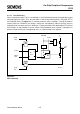
MCS03227
XTAL1
XTAL2
External
Clock
V
CC
Signal
N.C.
C515