
User`s manual

Semiconductor Group 6-49
On-Chip Peripheral Components
C515
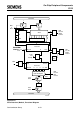
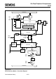
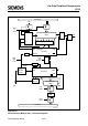
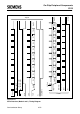
Figure 6-24
Serial Interface, Mode 0, Functional Diagram
MCS02101
Internal Bus
1
SBUF
Zero Detector
D
S
CLK
Q
Shift
Send
1
TX Control
Start
TX Clock
TI
RX Control
Start
RI
Receive
Shift
Serial
Port
Interrupt
Input Shift Register
SBUF
Internal Bus
Write
to
SBUF
Shift
Load
SBUF
Read
SBUF
RXD
P3.0 Alt.
Output
Function
Function
Output
P3.1 Alt.
TXD
1
Shift
Clock
&
REN
RI
S6
RX Clock
Function
Input
P3.0 Alt.
RXD
01 111111
&
&
Shift
Baud
Rate
Clock
_
<
_
<
Baud Rate
Clock