AirPrime HL7528 Product Technical Specification 4116873 10.
Product Technical Specification Important Notice Due to the nature of wireless communications, transmission and reception of data can never be guaranteed. Data may be delayed, corrupted (i.e., have errors) or be totally lost.
Product Technical Specification Patents This product may contain technology developed by or for Sierra Wireless Inc. This product is manufactured or sold by Sierra Wireless Inc. or its affiliates under one or more patents licensed from MMP Portfolio Licensing. Copyright © 2017 Sierra Wireless. All rights reserved. Trademarks Sierra Wireless®, AirPrime®, AirLink®, AirVantage®, WISMO®, ALEOS® and the Sierra Wireless and Open AT logos are registered trademarks of Sierra Wireless, Inc.
Product Technical Specification Document History Version Date Updates 1.0 July 20, 2015 Creation September 11, 2015 Updated: • Table 2 AirPrime HL7528 Features • Table 5 Pad Definition • Table 7 Current Consumption • Table 31 Ordering Information 2.0 November 25, 2015 Updated: • Table 6 Power Supply • 5.1 Power-Up Sequence 3.0 December 18, 2015 Removed dual SIM 4.0 February 11, 2016 Updated: • 3.10 POWER-ON Signal (PWR_ON_N) • 5.2 Module Switch-Off 4.
Contents 1. INTRODUCTION .................................................................................................. 9 1.1. Common Flexible Form Factor (CF3) ................................................................................ 9 1.2. Physical Dimensions ......................................................................................................... 9 1.3. General Features ........................................................................................................
Product Technical Specification 3.16.3. TX_ON Indicator (TX_ON) .......................................................................................31 4. MECHANICAL DRAWINGS ............................................................................... 32 5. DESIGN GUIDELINES ....................................................................................... 35 5.1. Power-Up Sequence .......................................................................................................35 5.2.
List of Figures Figure 1. AirPrime HL7528 Architecture Overview ......................................................................... 11 Figure 2. AirPrime HL7528 Mechanical Overview .......................................................................... 12 Figure 3. Pad Configuration ............................................................................................................ 19 Figure 4. PCM Master Mode Timing Waveform ..........................................................
List of Tables Table 1. Supported Bands/Connectivity .......................................................................................... 9 Table 2. AirPrime HL7528 Features .............................................................................................. 10 Table 3. ESD Specifications .......................................................................................................... 12 Table 4. AirPrime HL7528 Environmental Specifications ...................................
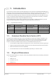
1. Introduction This document is the Product Technical Specification for the AirPrime HL7528 Embedded Module. It defines the high-level product features and illustrates the interfaces for these features. This document is intended to cover the hardware aspects of the product, including electrical and mechanical. The AirPrime HL7528 belongs to the AirPrime HL Series from Essential Connectivity Module family.
Product Technical Specification 1.3. Introduction General Features The table below summarizes the AirPrime HL7528 features. Table 2. AirPrime HL7528 Features Feature Description • Physical • • • Small form factor (146-pad solderable LGA pad) – 23mm x 22mm x 2.5mm (nominal) Complete body shielding RF connection pads (RF main interface) Baseband signals connection Electrical Single or double supply voltage (VBATT and VBATT_PA) – 3.2V – 4.
Product Technical Specification Introduction Feature Description RTC Real Time Clock (RTC) with calendar 1.4. Architecture The figure below presents an overview of the AirPrime HL7528’s internal architecture and external interfaces.
Product Technical Specification • 1x – TX ON • 1x – ADC • 1x – PCM 1.6. Introduction Connection Interface The AirPrime HL7528 module is an LGA form factor device. All electrical and mechanical connections are made through the 146 Land Grid Array (LGA) pads on the bottom side of the PCB. Figure 2. AirPrime HL7528 Mechanical Overview The 146 pads have the following distribution: • 66 inner signal pads, 1x0.5mm, pitch 0.8mm • 1 reserved test point (do not connect), 1.
Product Technical Specification 1.8. Introduction Environmental and Certifications 1.8.1. Environmental Specifications The environmental specification for both operating and storage conditions are defined in the table below. Table 4.
Product Technical Specification 1.9. [1] Introduction References AirPrime HL Series Customer Process Guidelines Reference Number: 4114330 [2] AirPrime HL7528 AT Commands Interface Guide Reference Number: 4116843 4116873 Rev 10.
2. Pad Definition AirPrime HL7528 pads are divided into 2 functional categories. • Core functions and associated pads cover all the mandatory features for M2M connectivity and will be available by default across all CF 3 family of modules. These Core functions are always available and always at the same physical pad locations. A customer platform using only these functions and associated pads is guaranteed to be forward and/or backward compatible with the next generation of CF3 modules.
Product Technical Specification Pad Definition Pad # Signal Name Function I/O Active Low/High Power Supply Domain Recommendation for Unused Pads Type 11 RESET_IN_N Input reset signal I L 1.8V Left Open Core Connect to test point Extension Connect to test point Extension USB Data Negative (Low / Full Speed) 3.
Product Technical Specification Pad Definition Power Supply Domain Recommendation for Unused Pads Type I 1.8V Left Open Extension PCM sync out I/O 1.8V Left Open Extension PCM_CLK PCM clock I/O 1.8V Left Open Extension 37 GND Ground 0V 0V Mandatory connection Core 38 NC Not Connected (Reserved for future use) Left Open Not connected 39 GND Ground 0V 0V Mandatory connection Core 40 GPIO7 General purpose input/output I/O 1.
Product Technical Specification Pad Definition Power Supply Domain Recommendation for Unused Pads Type 1.8V Left Open Extension 1.8V Mandatory connection Core 2.3V Left Open Core I 3.2V (min) 3.7V (typ) 4.5V (max) Mandatory connection Core Power supply (refer to section 3.1 Power Supply for more information) I 3.2V (min) 3.7V (typ) 4.5V (max) Mandatory connection Core VBATT Power supply I 3.2V (min) 3.7V (typ) 4.
Product Technical Specification Pad Configuration (Top View, Through Module) JTAG_RESET JTAG_TCK JTAG_TDO JTAG_TMS JTAG_TRST 167 242 241 240 239 238 237 236 JTAG_TDI 168 JTAG_RTCK NC NC USB_VBUS NC NC USB_D+ USB_DRESET_IN_N GPIO2 / TRACE_DATA2 UART1_DSR / TRACE_DATA0 UART1_DCD / TRACE_DATA1 UART1_DTR UART1_RX UART1_TX UART1_CTS UART1_RTS UART1_RI / TRACE_DATA3 GPIO1 2.1.
3. Detailed Interface Specifications Note: If not specified, all electrical values are given for VBATT=3.7V and an operating temperature of 25°C. For standard applications, VBATT and VBATT_PA must be tied externally to the same power supply. For some specific applications, AirPrime HL7528 module supports separate VBATT and VBATT_PA connection if requirements below are fulfilled. 3.1. Power Supply The AirPrime HL7528 module is supplied through the VBATT signal with the following characteristics. Table 6.
Product Technical Specification 3.3. Detailed Interface Specifications VGPIO The VGPIO output can be used to: • Pull-up signals such as I/Os • Supply the digital transistors driving LEDs The VGPIO output is available when the AirPrime HL7528 module is switched ON. Table 8. VGPIO Electrical Characteristics Parameter Minimum Typical Maximum Remarks Voltage level (V) 1.7 1.8 1.9 Both active mode and sleep mode Current capability (mA) - - 50 Rise Time (ms) - - 1.5 3.4.
Product Technical Specification Detailed Interface Specifications Table 10. UIM1 Pad Description Pad # Signal Name Description 26 UIM1_VCC 1.8V/3V SIM1 Power supply 27 UIM1_CLK 1.8V/3V SIM1 Clock 28 UIM1_DATA 1.8V/3V SIM1 Data 29 UIM1_RESET 1.8V/3V SIM1 Reset 64 UIM1_DET UIM1 Detection Table 11. Multiplex GPIO3 Electrical Characteristics of UIM1 Parameter Minimum Typical Maximum Remarks UIM1 Interface Voltage (V) (VCC, CLK, IO, RST) - 2.9 - - 1.
Product Technical Specification 3.7. Detailed Interface Specifications Electrical Information for Digital I/O The table below enumerates the electrical characteristics of the following digital interfaces: • UART • GPIOs • JTAG • RESET Table 13.
Product Technical Specification 3.9. Detailed Interface Specifications Main Serial Link (UART1) The main serial link (UART1) is used for communication between the AirPrime HL7528 module and a PC or host processor. It consists of a flexible 8-wire serial interface that complies with RS-232 interface. The supported baud rates of the UART1 are 300, 1200, 2400, 4800, 9600, 19200, 38400, 57600, 115200, 230400, 460800, 500000, 750000, 921600, 1843200, 3000000 and 3250000 bit/s.
Product Technical Specification Table 16. Detailed Interface Specifications PWR_ON_N Electrical Characteristics Parameter Minimum Input Voltage-Low (V) Typical Maximum - 0.51 Input Voltage-High (V) 1.33 - 2.2 Power-up period (ms) from PWR_ON_N falling edge 2000 - - PWR_ON_N assertion time (ms) 25 Note: As PWR_ON_N is internally pulled up with 100kΩ, an open collector or open drain transistor must be used for ignition.
Product Technical Specification Detailed Interface Specifications 3.12. Analog to Digital Converter (ADC1) One Analog to Digital Converter input, ADC1, is provided by the AirPrime HL7528 module. This converter is a 10-bit resolution ADC ranging from 0 to 1.2V. The following table describes the pad description of the ADC interface. Table 18.
Product Technical Specification Detailed Interface Specifications 3.14. PCM The Digital Audio (PCM) Interface allows connectivity with standard audio peripherals. It can be used, for example, to connect an external audio codec. The programmability of this interface allows addressing a large range of audio peripherals.
Product Technical Specification Detailed Interface Specifications T = corresponds to the audio sampling rate (48KHz, 44.1KHz, 32KHz, 24KHz, 22.05KHz, 16KHz, 12KHz, 11.025KHz and 8KHz) and to the frame rate length (17 bit, 18 bit, 32 bit, 48 bit or 64 bit). tCP = 9.6ns (clock period test condition) The following figure shows the PCM timing waveform. t1 t2 t3 PCM_CLK t4 t5 PCM_SYNC t7 PCM_OUT t6 0 15 13 14 t8 PCM_IN Figure 4.
Product Technical Specification Detailed Interface Specifications T = corresponds to the audio sampling rate (48KHz, 44.1KHz, 32KHz, 24KHz, 22.05KHz, 16KHz, 12KHz, 11.025KHz and 8KHz) and to the frame rate length (17 bit, 18 bit, 32 bit, 48 bit or 64 bit). tCP = 9.6ns (clock period test condition) The following figure shows the PCM slave mode timing waveform. t1 t2 PCM_CLK t3 t4 t5 PCM_SYNC t7 PCM_OUT 0 t6 15 13 14 t8 PCM_IN Figure 5.
Product Technical Specification Detailed Interface Specifications 3.15.2. JTAG The JTAG interface provides debug access to the core of the HL7528. These JTAG signals are accessible through solder-able test points. Table 25.
Product Technical Specification Detailed Interface Specifications 3.16.2. RF Performances RF performances are compliant with 3GPP recommendation TS 36.101. Table 28. Conducted RX Sensitivity (dBm) Frequency Band Primary (Typical) Secondary (Typical) SIMO (Typical) LTE B1 Full RB; BW: 20 MHz* -93.3 -93.3 -94.3 LTE B3 Full RB; BW: 20 MHz* -90.3 -90.3 -91.3 LTE B5 Full RB; BW: 10 MHz* -94.3 -94.3 -95.3 LTE B7 Full RB; BW: 20 MHz* -91.3 -91.3 -92.
4. Mechanical Drawings Figure 7. 4116873 AirPrime HL7528 Mechanical Drawing Rev 10.
Product Technical Specification Figure 8. 4116873 Mechanical Drawings AirPrime HL7528 Dimensions Drawing Rev 10.
Product Technical Specification Figure 9. 4116873 Mechanical Drawings AirPrime HL7528 Footprint Rev 10.
5. Design Guidelines 5.1. Power-Up Sequence Apply a low-level logic to the PWR_ON_N pad (pad 59); within approximately 25ms, VGPIO will appear to be at 1.8V. Either UART1 or the USB interface could be used to send AT commands. The AT command interface is available in about 7 seconds after PWR_ON_N for either UART1 or USB. When using UART1, the AT command interface is available after the transition of UART1_CTS from high to low level.
Product Technical Specification 5.2. Design Guidelines Module Switch-Off AT command AT+CFUN enables the user to properly switch the AirPrime HL7528 module off. AT+CFUN=0 Module is ON PWR_ON_N Interval pull-up to 1V8 Module is OFF 2 secs VGPIO Figure 12. Power OFF Sequence for PWR_ON_N, VGPIO Note: PWR_ON_N is internally pulled up by 100kΩ to 1.8V. 5.3. Emergency Power OFF If required, the module can be switched off by controlling the RESET_IN_N pad (pad 11).
Product Technical Specification 5.4.2. Design Guidelines Using USB Use AT+KSLEEP=1 to allows the module to automatically enter sleep mode while the USB interface is in use. 5.5. Power Supply Design The AirPrime HL7528 module should not be supplied with voltage over 4.5V even temporarily or however briefly. If the system’s main board power supply unit is unstable or if the system’s main board is supplied with over 4.
Product Technical Specification Design Guidelines UIM1_VCC UIM1_CLK UIM1_RESET UIM1_DATA UIM1_DET UIM1_VCC 1 VCC GND 5 UIM1_RESET 2 RST VPP 6 3 CLK I/O 7 4 C4 C8 8 UIM1_CLK UIM1_DATA 1KΩ UIM1_DET Figure 14. 5.7. DNI SW_B 10 1nF 9 SW_A 100KΩ 1K 1K 100nF DNI VGPIO EMC and ESD Components Close to the SIM ESD Guidelines for USB When the USB interface is externally accessible, it is required to have ESD protection on the USB_VBUS, USB_D+ and USB_D- signals. Figure 15.
Product Technical Specification 5.8. Design Guidelines Radio Integration The AirPrime HL7528 is equipped with an external antenna. A 50Ω line matching circuit between the module, the customer’s board and the RF antenna is required, for the GSM feed path, as shown in the example below. Antenna Detection 15kΩ 1% VGPIO 100kΩ 1% ADC1 7.5kΩ 1% GPIO5 22pF HL7528 33kΩ 1% 47nH 2.2kΩ 1% Antenna TBD RF_MAIN TBD Figure 16.
6. X-Ray Exposure X-ray exposure results in an undesirable shift in programmed bit threshold voltage of the Flash memory. As a result, Sierra Wireless recommends avoiding any X-ray exposure during customer manufacturing process to ensure software integrity and long-term reliability.
7. Ordering Information Table 31. Ordering Information Model Name Description Part Number HL7528 HL7528 embedded module Contact Sierra Wireless for the latest SKU DEV-KIT HL Series Development Kit 6000620 4116873 Rev 10.
8.
Product Technical Specification Terms and Abbreviations Abbreviation Definition RF Radio Frequency RFI Radio Frequency Interference RMS Root Mean Square RST Reset RTC Real Time Clock RX Receive SCL Serial Clock SDA Serial Data SIM Subscriber Identification Module SMD Surface Mounted Device/Design SPI Serial Peripheral Interface SW Software PSRAM Pseudo Static RAM TBC To Be Confirmed TBD To Be Defined TP Test Point TX Transmit TYP Typical UART Universal Asynchronous R