
User Guide


ATA AND TRUE IDE REGISTER DECODING SSD-CXXX(I)-3150 DATA SHEET
SILICONSYSTEMS PROPRIETARY
This document and the information contained within it is confidential and proprietary to SiliconSystems, Inc.
All unauthorized use and/or reproduction is prohibited.
3150C-10DSR PAGE 44 FEBRUARY 2, 2009
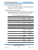
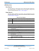
PRIMARY AND SECONDARY I/O MAPPED REGISTER DECODING
Table 32: Primary and Secondary I/O Mapped Register Decoding
Reg# A10
A9:A4
Primary
A9:A4
Secondary
A3 A2 A1 A0 IORD# = L IOWR# = L
0 X 1Fxh 17xh 0 0 0 0 Even Data
Read
Even Data
Write
0 X 1Fxh 17xh 0 0 0 1 Error Feature
0 X 1Fxh 17xh 0 0 1 0 Sector
Count
Sector
Count
0 X 1Fxh 17xh 0 0 1 1 Sector
Number
Sector
Number
0 X 1Fxh 17xh 0 1 0 0 Cylinder
Low
Cylinder
Low
0 X 1Fxh 17xh 0 1 0 1 Cylinder
High
Cylinder
High
0 X 1Fxh 17xh 0 1 1 0 Drive/Head Drive/Head
0 X 1Fxh 17xh 0 1 1 1 Status Command
0 X 3Fxh 37xh 0 1 1 0 Alternate
Status
Device
Control
0 X 3Fxh 37xh 0 1 1 1 Drive
Address
Reserved