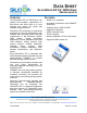
DATA SHEET SILICONDRIVE EP 2.5" PATA DRIVE SSD-DXXX(I)-4210 OVERVIEW FEATURES The SiliconDrive EP 2.5" PATA Drive is an optimal time-to-market replacement for hard drives and flash cards or in host systems that require low power and scalable storage solutions. • RoHS 6 of 6 compliant • Integrated PowerArmor and SiSMART technology • Capacity range: 16GB to 64GB • Supports 5V interface • MTBF 4,000,000 hours • ATA-5 compliant • Industry standard 2.
REVISION HISTORY SSD-DXXX(I)-4210 DATA SHEET REVISION HISTORY Document No. Release Date Changes 4210D-03DSR February 2, 2009 4210D-02DSR 4210D-01DSR PRELIMINARY 4210D-00DSR PRELIMINARY December 15, 2008 September 25, 2008 Updated: • "System Reliability" table and changed the name to "Reliability." • "Related Documentation" table. Added: • “Projected Operational Life Span.” External release with internal updates. Internal updates. September 16, 2008 Initial internal release.
TABLE OF CONTENTS SSD-DXXX(I)-4210 DATA SHEET TABLE OF CONTENTS Overview .......................................................................................................................... i Features ........................................................................................................................... i Revision History..............................................................................................................II List of Figures ................................
TABLE OF CONTENTS SSD-DXXX(I)-4210 DATA SHEET ATA Registers............................................................................................................... 28 Data Register ............................................................................................................. 28 Error Register ............................................................................................................. 28 Feature Register.................................................................
TABLE OF CONTENTS SSD-DXXX(I)-4210 DATA SHEET Read Long Sector(s) — 22h, 23h......................................................................... 57 Read Verify Sector(s) — 40h, 41h ....................................................................... 58 Seek — 7Xh ......................................................................................................... 59 Set Features — EFh.............................................................................................
LIST OF FIGURES SSD-DXXX(I)-4210 DATA SHEET LIST OF FIGURES Figure 1: Physical Dimensions......................................................................................... 1 Figure 2: Pin Locations .................................................................................................... 2 Figure 3: Jumper Settings................................................................................................ 2 Figure 4: True IDE PIO Mode Read/Write Access Timing Diagram .................
LIST OF TABLES SSD-DXXX(I)-4210 DATA SHEET LIST OF TABLES Table 1: System Performance ......................................................................................... 3 Table 2: System Power Requirements ............................................................................ 3 Table 3: Reliability............................................................................................................ 4 Table 4: Operational Life Span ........................................................
LIST OF TABLES SSD-DXXX(I)-4210 DATA SHEET Table 28: ATA Command Set ........................................................................................ 40 Table 29: Check Power Mode — 98h, E5h.................................................................... 42 Table 30: Executive Drive Diagnostic — 90h................................................................. 43 Table 31: Format Track — 50h ......................................................................................
LIST OF TABLES SSD-DXXX(I)-4210 DATA SHEET Table 57: Request Sense — 03h................................................................................... 71 Table 58: Extended Error Codes ................................................................................... 71 Table 59: Translate Sector — 87h ................................................................................. 72 Table 60: Wear-Level — F5h.........................................................................................
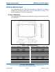
PHYSICAL SPECIFICATIONS SSD-DXXX(I)-4210 DATA SHEET PHYSICAL SPECIFICATIONS The SiliconDrive EP 2.5" PATA Drive products are offered in an industrystandard 2.5" PATA Drive form factor. See "Part Numbering" on page 77 for details regarding 2.5" PATA Drive capacities. PHYSICAL DIMENSIONS This section provides diagrams that describe the physical dimensions for the 2.5" PATA Drive.
PHYSICAL SPECIFICATIONS SSD-DXXX(I)-4210 DATA SHEET PIN LOCATIONS The following diagram identifies the pin locations of the 2.5" PATA Drive. Figure 2: Pin Locations JUMPER SETTINGS The following diagram defines the SiliconDrive EP 2.5" PATA Drive jumper settings. Figure 3: Jumper Settings SILICONSYSTEMS PROPRIETARY This document and the information contained within it is confidential and proprietary to SiliconSystems, Inc. All unauthorized use and/or reproduction is prohibited.
PRODUCT SPECIFICATIONS SSD-DXXX(I)-4210 DATA SHEET PRODUCT SPECIFICATIONS Note: All SiliconDrive EP 2.5" PATA Drive values quoted are typical at 25°C and nominal supply voltage.
PRODUCT SPECIFICATIONS SSD-DXXX(I)-4210 DATA SHEET RELIABILITY Table 3: Reliability MTBF (@ 25ºC) 4,000,000 hours Bit Error Rate <1 non-recoverable error in 1014 bits read PROJECTED OPERATIONAL LIFE SPAN Table 4: Operational Life Span SiliconDrive Part# Capacity Service Life* GB Written per Day SSD-D64G-4210 64GB 17.9 Years @ 978.5GB SSD-D32G-4210 SSD-D16G-4210 32GB 16GB 9.0 Years 4.5 Years @ 978.5GB @ 978.5GB * There are unlimited read cycles.
PRODUCT SPECIFICATIONS SSD-DXXX(I)-4210 DATA SHEET PRODUCT CAPACITY SPECIFICATIONS Table 5: Product Capacity Specifications Product Capacity Capacity (Bytes) 16GB 32GB 64GB Number of Sectors Number of Number of Number Sectors/ Cylinders of Heads Track 16,391,208,960 32,014,080 16,383* 32,782,417,920 64,028,160 16,383* 65,564,835,840 128,056,320 16,383* 16 16 16 63 63 63 * = All IDE drives 8GB and larger use 16383 cylinders, 16 heads, and 63 sectors/track due to interface restrictions.
ELECTRICAL SPECIFICATION SSD-DXXX(I)-4210 DATA SHEET ELECTRICAL SPECIFICATION PIN ASSIGNMENTS The following table describes the SiliconDrive EP 2.5" PATA Drive 44-pin IDE connector signals.
ELECTRICAL SPECIFICATION SSD-DXXX(I)-4210 DATA SHEET SIGNAL DESCRIPTIONS Table 8: Signal Descriptions Signal Name Pin(s) Type Description A2-A0 36, 33, 35 I -CS0,-CS1 37, 38 I -CSEL 28 I Address Inputs. These signals are asserted by the host to access the task registers in the device. In the true IDE mode, -CS0 is the chip select for the task file registers while -CS1 is used to select the Alternate Status register and the Device Control register. Cable Select.
ELECTRICAL SPECIFICATION SSD-DXXX(I)-4210 DATA SHEET Table 8: Signal Descriptions (Continued) Signal Name Pin(s) Type Description DMARQ 21 O DMA Request. This signal is used for DMA transfers between the host and device. DMARQ is asserted by the device when the device is ready to transfer data to/from the host. The direction of data transfer is controller by -IORD and -IOWR. This signal is used in a handshake manner with DMACK (i.e.
ELECTRICAL SPECIFICATION SSD-DXXX(I)-4210 DATA SHEET Table 8: Signal Descriptions (Continued) Signal Name Pin(s) Type Description DMARQ# (UDMA protocol active) GND INTRQ 2, 19, 22, 24, 26, 30, 40, 43 31 O This signal is a DMA request that is used for DMA data transfers between the host and device. This signal is asserted by the device when it is ready to transfer data to or from the host. For Multiword DMA transfers, the direction of data transfer is controlled by -IORD and -IOWR.
ELECTRICAL SPECIFICATION SSD-DXXX(I)-4210 DATA SHEET Table 8: Signal Descriptions (Continued) Signal Name Pin(s) Type Description IORDY (True IDE mode) -IORD (True IDE mode) 27 I I/O Channel Ready. The signal is negated to extend the host transfer cycle of any host register access. 25 I Device I/O Read. This is the read strobe signal from the host. The falling edge of IORD enables data from the device onto the data bus. The rising edge of IORD latches data at the host.
ELECTRICAL SPECIFICATION SSD-DXXX(I)-4210 DATA SHEET Table 8: Signal Descriptions (Continued) Signal Name Pin(s) Type Description HDSTROBE (UDMA write protocol active) When UDMA mode DMA write is active in all modes, this signal is the data-out strobe generated by the host. Both the rising and falling edge of HSTROBE cause data to be latched by the device. The host may stop generating HSTROBE edges to pause an UDMA data-out burst. Key. Reserved for the Connector Key.
ELECTRICAL SPECIFICATION SSD-DXXX(I)-4210 DATA SHEET DC CHARACTERISTICS Table 10: DC Characteristics 5V ± 10% Symbol Parameter Units Minimum Maximum ILI Input Leakage *(1) Current - 10 μA ILO Output Leakage *(1) Current - 10 μA ICCR ICC Read Current - 100 mA ICCW ICC Write Current - 200 mA ICCS ICC Standby Current - 15 mA SILICONSYSTEMS PROPRIETARY This document and the information contained within it is confidential and proprietary to SiliconSystems, Inc.
ELECTRICAL SPECIFICATION SSD-DXXX(I)-4210 DATA SHEET AC CHARACTERISTICS True IDE PIO Mode Read/Write Access Timing ADDR valid (A02, A01, A00, -CS0, -CS1) note 1) 1) (See note t0 t1 t2 t9 t8 t 2i -IORD / -IOWR Write Data (D15:D00) (See note 2) 2) (See note t3 t4 t5 t6 Read Data (D15:D00) (See note 2) 2) (See note t7 t 6z -IOCS16 (See note 3) IORDY (See note note 4, 4a)4-1) tA IORDY (See note note 4, 4b) 4-2) tC t RD IORDY (See note note 4, 4c)4-3) tB tC Figure 4: True IDE PIO Mode Re
ELECTRICAL SPECIFICATION SSD-DXXX(I)-4210 DATA SHEET Table 11: True IDE PIO Mode Read/Write Access Timing Symbol Item Mode 0 Mode 1 Mode 2 Mode 3 Mode 4 Mode 5 Mode 6 Note Units t0 Cycle Time (minimum) 600 383 240 180 120 100 80 1 ns t1 Address Valid to IORD/-IOWR Setup (minimum) 70 50 30 30 25 15 10 - ns t2 -IORD/-IOWR (minimum) 165 125 100 80 70 65 55 1 ns t2 -IORD/-IOWR (minimum) 290 register (8 bit) 290 290 80 70 65 55 1 ns t2i -IORD/-IOWR Recovery Time (mi
ELECTRICAL SPECIFICATION SSD-DXXX(I)-4210 DATA SHEET 3. The delay from the activation of -IORD or -IOWR until the state of IORDY is first sampled. If IORDY is inactive, then the host waits until IORDY is active before the PIO cycle can be completed. If the drive is not driving IORDY negated at tA after the activation of -IORD or -IOWR, then t5 must be met and tRD is not applicable.
ELECTRICAL SPECIFICATION SSD-DXXX(I)-4210 DATA SHEET Table 12: True IDE Multiword DMA Read/Write Access Timing Symbol Item Mode 0 Mode 1 Mode 2 Mode 3 Mode 4 Note Units tO Cycle Time (minimum) 480 tD -IORD/-IOWR Asserted Width (minimum) tE 150 120 100 80 1 ns 215 80 70 65 55 1 ns -IORD Data Access (maximum) 150 60 50 50 45 - ns tF -IORD Data Hold (minimum) 5 5 5 5 5 - ns tG -IORD/-IOWR Data Setup (minimum) 100 30 20 15 10 - ns tH -IOWR Data Hold (minimum) 2
ELECTRICAL SPECIFICATION SSD-DXXX(I)-4210 DATA SHEET Ultra DMA Data Burst Timing Requirements The following figures and table describe the requirements for the Ultra DMA (UDMA) data burst timing.
ELECTRICAL SPECIFICATION SSD-DXXX(I)-4210 DATA SHEET t2CYC tCYC tCYC t2CYC DSTROBE at device tDVH tDVS tDVH tDVS tDVH DD(15:0) at device DSTROBE at host tDH tDS tDH tDS tDH DD(15:0) at host Figure 7: Sustained UDMA Data-In Burst Note: DD(15:0) and DSTROBE signals are shown at both the host and the device to emphasize that the cable settling time as well as cable propagation delay does not allow the data signals to be considered stable at the host until some time after they are driven by the
ELECTRICAL SPECIFICATION SSD-DXXX(I)-4210 DATA SHEET DMARQ (device) tMLI DMACK(host) tACK tLI tLI STOP (host) tACK tLI HDMARDY(host) tSS DSTROBE (device) tIORDYZ tZAH tAZ tDVS DD(15:0) tDVH CRC tACK DA0, DA1, DA2, CS0-, CS1- Figure 9: Device Terminating a UDMA Data-In Burst Note: The definitions for the DIOW-:STOP, DIOR-:HDMARDY-:HSTROBE, and IORDY:DDMARDY-:DSTROBE signal lines are no longer in effect after DMARQ and DMACK are negated.
ELECTRICAL SPECIFICATION SSD-DXXX(I)-4210 DATA SHEET DMARQ (device) tLI tMLI DMACK(host) tZAH tAZ tRP tACK STOP (host) tACK HDMARDY(host) tRFS tLI tMLI tIORDYZ DSTROBE (device) tDVS DD(15:0) tDVH CRC tACK DA0, DA1, DA2, CS0-, CS1- Figure 10: Host Terminating a UDMA Data-In Burst Note: The definitions for the DIOW-:STOP, DIOR-:HDMARDY-:HSTROBE, and IORDY:DDMARDY-:DSTROBE signal lines are no longer in effect after DMARQ and DMACK are negated.
ELECTRICAL SPECIFICATION SSD-DXXX(I)-4210 DATA SHEET DMARQ (device) tUI DMACK(host) tACK tENV STOP (host) tZIORDY tLI tUI DDMARDY(device) tACK HSTROBE (host) tDVS tDVH DD(15:0) (host) tACK DA0, DA1, DA2, CS0-, CS1- Figure 11: Initiating a UDMA Data-Out Burst Note: The definitions for the DIOW-:STOP, IORDY:DDMARDY:DSTROBE, and DIOR-:HDMARDY-:HSTROBE signal lines are not in effect until DMARQ and DMACK are asserted.
ELECTRICAL SPECIFICATION SSD-DXXX(I)-4210 DATA SHEET tRP DMARQ (device) DMACK(host) STOP (host) tSR DDMARDY(device) tRFS HSTROBE (host) DD(15:0) (host) Figure 13: Device Pausing a UDMA Data-Out Burst Notes: 1. The device may negate DMARQ to request termination of the UDMA burst no sooner than tRP after DDMARDY- is negated. 2. If the tSR timing is not satisfied, the host may receive zero, one, or two more data words from the host.
ELECTRICAL SPECIFICATION SSD-DXXX(I)-4210 DATA SHEET tLI DMARQ (device) tMLI DMACK(host) tLI tSS tACK STOP (host) tLI tIORDYZ DDMARDY(device) tACK HSTROBE (host) tDVS DD(15:0) (host) tDVH CRC tACK DA0, DA1, DA2, CS0-, CS1- Figure 14: Host Terminating a UDMA Data-Out Burst Note: The definitions for the DIOW-:STOP, IORDY:DDMARDY:DSTROBE, and DIOR-:HDMARDY-:HSTROBE signal lines are no longer in effect after DMARQ and DMACK are negated.
ELECTRICAL SPECIFICATION SSD-DXXX(I)-4210 DATA SHEET DMARQ (device) DMACK(host) tLI tMLI tACK STOP (host) tRP tIORDYZ DDMARDY(device) tRFS tMLI tLI tACK HSTROBE (host) tDVS DD(15:0) (host) tDVH CRC tACK DA0, DA1, DA2, CS0-, CS1- Figure 15: Device Terminating a UDMA Data-Out Burst Note: The definitions for the DIOW-:STOP, IORDY:DDMARDY:DSTROBE, and DIOR-:HDMARDY-:HSTROBE signal lines are no longer in effect after DMARQ and DMACK are negated.
ELECTRICAL SPECIFICATION SSD-DXXX(I)-4210 DATA SHEET Table 13: UDMA Data Burst Timing Requirements (Continued) Mode 0 Mode 1 Mode 2 Mode 3 Mode 4 Symbol Comment (see Notes 1 and 2) Units Min. Max. Min. Max. Min. Max. Min. Max. Min. Max. tDVS 70 - 48 - 30 - 20 - 6 - Data valid setup time at ns sender (from data valid until STROBE edge) (see Note 4). tDVH 6 - 6 - 6 - 6 - 6 - Data valid hold time at sender (from STROBE edge until data may become invalid) (see Note 4).
ELECTRICAL SPECIFICATION SSD-DXXX(I)-4210 DATA SHEET Table 13: UDMA Data Burst Timing Requirements (Continued) Mode 0 Mode 1 Mode 2 Mode 3 Mode 4 Symbol tSS Min. Max. Min. Max. Min. Max. Min. Max. Min. Max. 50 - - 50 - 50 50 - 50 - Comment (see Notes 1 and 2) Time from STROBE edge to negation of DMARQ or assertion of STOP (when the sender terminates a burst). Units ns Notes: 1. Timing parameters are measured at the connector of the sender or receiver to which the parameter applies.
ATA AND TRUE IDE REGISTER DECODING SSD-DXXX(I)-4210 DATA SHEET ATA AND TRUE IDE REGISTER DECODING SiliconDrive EP can be configured as either a a memory-mapped or an an I/O devices. As noted earlier, communication to and from the drive is accomplished using the ATA Command Block. TASK FILE REGISTER SPECIFICATION The Task File registers are used for reading and writing the storage data in the SiliconDrive EP. The decoded addresses are as shown in the following table.
ATA REGISTERS SSD-DXXX(I)-4210 DATA SHEET ATA REGISTERS DATA REGISTER The Data register is a 16-bit register used to transfer data blocks between the host and drive buffers. The register may set to 8-bit mode by using the Set Features Command defined in "Seek — 7Xh" on page 59. ERROR REGISTER The Error register contains the error status, if any, generated from the last executed ATA command. The contents are qualified by the ERR bit being set in "Status Register" on page 35.
ATA REGISTERS SSD-DXXX(I)-4210 DATA SHEET FEATURE REGISTER The Feature register is command-specific and used to enable and disable interface features. This register supports only either odd or even byte data transfers. Table 16: Feature Register Operation D7 D6 D5 Read/Write D4 D3 D2 D1 D0 Feature Byte SILICONSYSTEMS PROPRIETARY This document and the information contained within it is confidential and proprietary to SiliconSystems, Inc. All unauthorized use and/or reproduction is prohibited.
ATA REGISTERS SSD-DXXX(I)-4210 DATA SHEET SECTOR COUNT REGISTER The Sector Count register is used to read or write the sector count of the data for which an ATA transfer has been made. Table 17: Sector Count Register Operation D7 D6 D5 Read/Write Default Value D4 D3 D2 D1 D0 0 0 1 Sector Count 0 0 0 0 0 SILICONSYSTEMS PROPRIETARY This document and the information contained within it is confidential and proprietary to SiliconSystems, Inc.
ATA REGISTERS SSD-DXXX(I)-4210 DATA SHEET SECTOR NUMBER REGISTER The Sector Number register is set by the host to specify the starting sector number associated with the next ATA command to be executed. Following a qualified ATA command sequence, the device sets the register value to the last sector read or written as a result of the previous AT command.
ATA REGISTERS SSD-DXXX(I)-4210 DATA SHEET CYLINDER LOW REGISTER The Cylinder Low register is set by the host to specify the cylinder number low byte. Following an ATA command, the content of the register is written by the device, identifying the cylinder number low byte. In LBA mode, the 8-bit register maintains the contents of the Logical Block number address bits A15:A08.
ATA REGISTERS SSD-DXXX(I)-4210 DATA SHEET CYLINDER HIGH REGISTER The Cylinder High register is set by the host to specify the cylinder number high byte. Following an ATA command, the content of the register is set internally by the device, identifying the cylinder number high byte. In LBA mode, the 8-bit register maintains the contents of the Logical Block number address bits A23:A16.
ATA REGISTERS SSD-DXXX(I)-4210 DATA SHEET DRIVE/HEAD REGISTER The Drive/Head register is used by the host and the device to select the type of addressing (CHS or LBA), the drive letter, and either bits 3-0 of the head number in CHS mode or logical block number bits 27-24 in LBA mode.
ATA REGISTERS SSD-DXXX(I)-4210 DATA SHEET STATUS REGISTER The Status register provides the device’s current status to the host. The status register is an 8-bit read-only register. When the contents of the register are read by the host, the IREQ# bit is cleared. Table 22: Status Register Operation D7 D6 D5 D4 D3 D2 D1 D0 Read/Write BSY DRDY DWF DSC DRQ CORR IDX ERR 0 0 0 0 0 0 0 0 Default Value Bit(s) Description 7 Busy (BSY).
ATA REGISTERS SSD-DXXX(I)-4210 DATA SHEET COMMAND REGISTER The Command register specifies the ATA command code being issued to the drive by the host. Execution of the command begins immediately following the issuance of the command register code by the host. Table 23: Command Register Operation Read/Write D7 D6 D5 D4 D3 D2 D1 D0 ATA Command Code See "ATA Command Block and Set Description" on page 40 for a listing of the supported ATA commands.
ATA REGISTERS SSD-DXXX(I)-4210 DATA SHEET ALTERNATE STATUS REGISTER The Alternate Status register is a read-only register indicating the status of the device, following the previous ATA command. See "Status Register" on page 35 for specific details.
ATA REGISTERS SSD-DXXX(I)-4210 DATA SHEET DEVICE CONTROL REGISTER The Device Control register is used to control the interrupt request and issue ATA software resets. Table 25: Device Control Register Operation Write D7 D6 D5 D4 D3 D2 D1 D0 - - - - 1 SRST nIEN 0 Bit(s) Description 7-4 Reserved bits. 3 2 1 Always set to 1. Software Reset (SRST). When set, resets the ATA software. Interrupt Enable (nIEN). When set, device interrupts are disabled.
ATA REGISTERS SSD-DXXX(I)-4210 DATA SHEET DEVICE ADDRESS REGISTER The Device Address register is used to maintain compatibility with ATA disk drive interfaces. Table 26: Device Address Register Operation D7 Read/Write - Default Value 0 D6 D5 D4 D3 D2 D1 D0 nWTG nHS3 nHS2 nHS1 nHS0 nDS1 nDS0 0 1 1 1 1 1 0 Bit(s) Description 7 6 5-2 Reserved bit. Write Gate (nWTG). Low when a write to the device is in process. nHS3 to nHS0. The negated binary address of the currently selected head.
ATA COMMAND BLOCK AND SET DESCRIPTION SSD-DXXX(I)-4210 DATA SHEET ATA COMMAND BLOCK AND SET DESCRIPTION In accordance with the ANSI ATA Specification, the device implements seven registers that are used to transfer instructions to the device by the host. These commands follow the ANSI standard ATA protocol. A description of the ATA command block is provided in the following table.
ATA COMMAND BLOCK AND SET DESCRIPTION SSD-DXXX(I)-4210 DATA SHEET Table 28: ATA Command Set (Continued) Class Command Name Command Code FR 1 1 1 1 1 1 1 1 1 1 1 1 1 2 1 2 3 3 22h, 23h 20h, 21h 40h, 41h 1Xh 03h 7Xh EFh C6h 99h, E6h 96h, E2h 94h, E0h 87h F5h E8h CAh 32h, 33h C5h CDh 2 2 3 Read Long Sector Read Sector(s) Read Verify Sector(s) Recalibrate Request Sense Seek Set Features Set Multiple Mode Set Sleep Mode Standby Standby Immediate Translate Sector Wear Level Write Buffer Write DMA* Write Lo
ATA COMMAND BLOCK AND SET DESCRIPTION SSD-DXXX(I)-4210 DATA SHEET Check Power Mode — 98h, E5h The Check Power Mode command verifies the device’s current power mode. When the device is configured for standby mode or is entering or exiting standby, the BSY bit is set, the Sector Count register set to 00h, and the BSY bit is cleared. In idle mode, BSY is set and the Sector Count register is set to FFh. The BSY bit is then cleared and an interrupt is issued.
ATA COMMAND BLOCK AND SET DESCRIPTION SSD-DXXX(I)-4210 DATA SHEET Executive Drive Diagnostic — 90h The Executive Drive Diagnostic performs an internal read write diagnostic test using (AA55h and 55AAh). If an error is detected in the read/write buffer, the Error register reports the appropriate diagnostic code.
ATA COMMAND BLOCK AND SET DESCRIPTION SSD-DXXX(I)-4210 DATA SHEET Format Track — 50h The Format Track command formats the common solid-state memory array.
ATA COMMAND BLOCK AND SET DESCRIPTION SSD-DXXX(I)-4210 DATA SHEET Identify Drive — ECh Issued by the host, the Identify Drive command provides 256 bytes of drive attribute data (i.e., sector size, count, and so on) The identify drive data structure is detailed in the following table.
ATA COMMAND BLOCK AND SET DESCRIPTION SSD-DXXX(I)-4210 DATA SHEET Identify Drive — Drive Attribute Data Table 33: Identify Drive — Drive Attribute Data Word Data Default Address Bytes Data Description 0 2 General configuration bit information 2 2 2 2 2 2 4 2 20 • 15: Non-magnetic disk • 14: Formatting speed latency permissible gap needed • 13: Track Offset option supported • 12: Data Strobe Offset option supported • 11: Over 0.
ATA COMMAND BLOCK AND SET DESCRIPTION SSD-DXXX(I)-4210 DATA SHEET Table 33: Identify Drive — Drive Attribute Data (Continued) Word Data Default Address Bytes Data Description 20 2 0001h 21 22 0001h 0004h 2 2 23-26 27-46 47 XXXXh XXXXh 8001h 8 40 2 48 49 0000h 0f00h 2 2 50 51 52 53 0000h 0200h 0000h 0007h 2 2 2 2 54 55 56 57-58 59 XXXXh XXXXh XXXXh XXXXh 010Xh 2 2 2 4 2 60-61 XXXXh 4 Buffer type • 0000h: Not specified • 0001h: A single-ported, single-sector buffer • 0002h: A dual-por
ATA COMMAND BLOCK AND SET DESCRIPTION SSD-DXXX(I)-4210 DATA SHEET Table 33: Identify Drive — Drive Attribute Data (Continued) Word Data Default Address Bytes Data Description 62 63 0000h 0007h 2 2 64 65 0003h 0078h 2 2 66 0078h 2 67 0078h 2 68 0078h 2 80 003Eh 2 88 001Fh 2 163 0002h 2 Single-word DMA modes supported • 2: Multiword DMA mode 2 supported • 1: Multiword DMA mode 1 supported • 0: Multiword DMA mode 0 supported 7-0: Advanced PIO modes supported 15-0: Multiword DMA cycl
ATA COMMAND BLOCK AND SET DESCRIPTION SSD-DXXX(I)-4210 DATA SHEET Idle — 97h, E3h When issued by the host, the device’s internal controller sets the BSY bit, enters the Idle mode, clears the BSY bit, and generates an interrupt. If the sector count is non-zero, it is interpreted as a timer count with each count being 5ms, and the automatic power-down mode is enabled. If the sector count is zero, the automatic power-down mode is disabled.
ATA COMMAND BLOCK AND SET DESCRIPTION SSD-DXXX(I)-4210 DATA SHEET Idle Immediate — 95h, E1h When issued by the host, the device’s internal controller sets the BSY bit, enters Idle Mode, clears the BSY bit, and issues an interrupt. The interrupt is issued whether or not the Idle mode is fully entered.
ATA COMMAND BLOCK AND SET DESCRIPTION SSD-DXXX(I)-4210 DATA SHEET Initialize Drive Parameters — 91h Initialize Drive Parameters allows the host to set the sector counts per track and the head counts per cylinder to 1 Fixed. Upon issuance of the command, the device sets the BSY bit and associated parameters, clears the BSY bit, and issues an interrupt.
ATA COMMAND BLOCK AND SET DESCRIPTION SSD-DXXX(I)-4210 DATA SHEET Recalibrate — 1Xh The Recalibrate command sets the cylinder low and high, head number to 0h, and sector number to 1h in CHS mode. In LBA mode (i.e., LBA = 1), the sector number is set to 0h.
ATA COMMAND BLOCK AND SET DESCRIPTION SSD-DXXX(I)-4210 DATA SHEET Read Buffer — E4h The Read Buffer command allows the host to read the contents of the sector buffer. When issued, the device sets the BSY bit and sets up the sector buffer data in preparation for the read operation. When the data is ready, the DRQ bit is set and the BSY bit in the Status register are set and cleared, respectively.
ATA COMMAND BLOCK AND SET DESCRIPTION SSD-DXXX(I)-4210 DATA SHEET Read DMA — C8h The Read DMA command allows the host to read data using the DMA transfer protocol. Note: This function does not apply to SiliconDrive EPs that have DMA disabled.
ATA COMMAND BLOCK AND SET DESCRIPTION SSD-DXXX(I)-4210 DATA SHEET Read Multiple — C4h The Read Multiple command executes similarly to the Read Sector command, with the exception that interrupts are issued only when a block containing the counts of sectors defined by the Set Multiple command is transferred.
ATA COMMAND BLOCK AND SET DESCRIPTION SSD-DXXX(I)-4210 DATA SHEET Read Sector — 20h, 21h The Read Sector command allows the host to read sectors 1 to 256 as specified in the Sector Count register. If the sector count is set to 0h, all 256 sectors of data are made available. When the command code is issued and the first sector of data has been transferred to the buffer, the DRQ bit is set.
ATA COMMAND BLOCK AND SET DESCRIPTION SSD-DXXX(I)-4210 DATA SHEET Read Long Sector(s) — 22h, 23h The Read Long Sector(s) command operates similarly to the Read Sector(s) command, with the exception that it transfers requested data sectors and ECC data. The long instruction ECC byte transfer for Long commands is a byte transfer at a fixed length of 4 bytes.
ATA COMMAND BLOCK AND SET DESCRIPTION SSD-DXXX(I)-4210 DATA SHEET Read Verify Sector(s) — 40h, 41h The Read Verify Sector(s) command operates similarly to the Read Sector(s) command, with the exception that is does not set the DRQ bit and does not transfer data to the host. When the requested sectors are verified, the onboard controller clears the BSY bit and issues an interrupt.
ATA COMMAND BLOCK AND SET DESCRIPTION SSD-DXXX(I)-4210 DATA SHEET Seek — 7Xh The Seek command seeks and picks up the head to the tracks specified in the task file. When the command is issued, the solid-state memory chips do not need to be formatted. After an appropriate amount of time, the DSC bit is set.
ATA COMMAND BLOCK AND SET DESCRIPTION SSD-DXXX(I)-4210 DATA SHEET Set Features — EFh The Set Features command allows the host to configure the feature set of the device according to the attributes listed in Table 46.
ATA COMMAND BLOCK AND SET DESCRIPTION SSD-DXXX(I)-4210 DATA SHEET Set Multiple Mode — C6h The Set Multiple Mode command allows the host to access the drive via Read Multiple and Write Multiple ATA commands. Additionally, the command sets the block count (i.e., the number of sectors within the block) for the Read/Write Multiple command. The sector count per block is set in the Sector Count register.
ATA COMMAND BLOCK AND SET DESCRIPTION SSD-DXXX(I)-4210 DATA SHEET Set Sleep Mode — 99h, E6h The Set Sleep Mode command allows the host to set the device in sleep mode. When the onboard controller transitions to sleep mode, it clears the BSY bit and issues an interrupt. The device interface then becomes inactive. Sleep mode can be exited by issuing either a hardware or software reset.
ATA COMMAND BLOCK AND SET DESCRIPTION SSD-DXXX(I)-4210 DATA SHEET Standby — 96h, E2h When the Standby command is issued by the host, it transitions the device into standby mode. If the Sector Count register is set to a value other than 0h, the Auto Powerdown function is enabled and the device returns to Idle mode.
ATA COMMAND BLOCK AND SET DESCRIPTION SSD-DXXX(I)-4210 DATA SHEET Standby Immediate — 94h, E0h When the Standby Immediate command is issued by the host, it transitions the device into standby mode.
ATA COMMAND BLOCK AND SET DESCRIPTION SSD-DXXX(I)-4210 DATA SHEET Write Buffer — E8h The Write Buffer command allows the host to rewrite the contents of the 512- byte data buffer with the wanted data.
ATA COMMAND BLOCK AND SET DESCRIPTION SSD-DXXX(I)-4210 DATA SHEET Write DMA — CAh The Write DMA command allows the host to write data using the DMA transfer protocol. Note: This function does not apply to SiliconDrive EPs that have DMA disabled.
ATA COMMAND BLOCK AND SET DESCRIPTION SSD-DXXX(I)-4210 DATA SHEET Write Multiple — C5h The Write Multiple command operates in the same manner as the Write Sector command. When issued, the device sets the BSY bit within 400ns and generates an interrupt at the completion of a transferred block of sectors. The DRQ bit is set at the beginning of a block transfer.
ATA COMMAND BLOCK AND SET DESCRIPTION SSD-DXXX(I)-4210 DATA SHEET Write Sector(s) — 30h, 31h The Write Sector(s) command writes from 1 to 256 sectors as specified in the Sector Count register. A sector count of 0 requests 256 sectors. When issued, the device sets the BSY bit within 400ns and generates an interrupt at the completion of a transferred block of sectors. The DRQ bit is set at the beginning of a block transfer.
ATA COMMAND BLOCK AND SET DESCRIPTION SSD-DXXX(I)-4210 DATA SHEET Write Long Sector(s) — 32h, 33h The Write Long Sector(s) command operates in the same manner as the Write Sector command — when issued, the device sets the BSY bit within 400ns and generates an interrupt at the completion of a transferred block of sectors. The DRQ bit is set at the beginning of a block transfer.
ATA COMMAND BLOCK AND SET DESCRIPTION SSD-DXXX(I)-4210 DATA SHEET Erase Sector(s) — C0h The Erase Sector(s) command is issued prior to the issuance of a Write Sector(s) or Write Multiple w/o Erase command.
ATA COMMAND BLOCK AND SET DESCRIPTION SSD-DXXX(I)-4210 DATA SHEET Request Sense — 03h The Request Sense command identifies the extended error codes generated by the preceding ATA command. The Request Sense command must be issued immediately following the detection of an error via the Error register.
ATA COMMAND BLOCK AND SET DESCRIPTION SSD-DXXX(I)-4210 DATA SHEET Translate Sector — 87h The Translate Sector command is not currently supported by the SiliconSystems’ SiliconDrive EP. If the host issues this command, the device responds with 0x00h in the data register.
ATA COMMAND BLOCK AND SET DESCRIPTION SSD-DXXX(I)-4210 DATA SHEET Wear-Level — F5h The Wear-Level command is supported as an NOP command for the purposes of backward compatibility with the ANSI AT attachment standard. This command sets the Sector Count register to 0x00h.
ATA COMMAND BLOCK AND SET DESCRIPTION SSD-DXXX(I)-4210 DATA SHEET Write Multiple w/o Erase — CDh The Write Multiple w/o Erase command functions identically to the Write Multiple command, with the exception that the implied pre-erase (i.e., Erase Sector(s) command) is not issued prior to writing the sectors.
ATA COMMAND BLOCK AND SET DESCRIPTION SSD-DXXX(I)-4210 DATA SHEET Write Sector(s) w/o Erase — 38h The Write Sector(s) w/o Erase command functions similar to the Write Sector command, with the exception that the implied pre-erase (i.e., Erase Sector(s) command) is not issued prior to writing the sectors.
ATA COMMAND BLOCK AND SET DESCRIPTION SSD-DXXX(I)-4210 DATA SHEET Write Verify — 3Ch The Write Verify command verifies each sector immediately after it is written. This command performs identically to the Write Sector(s) command, with the added feature of verifying each sector written.
SALES AND SUPPORT SSD-DXXX(I)-4210 DATA SHEET SALES AND SUPPORT To order or obtain information on pricing and delivery, contact your SiliconSystems Sales Representative. PART NUMBERING NOMENCLATURE The following table defines the SiliconDrive EP 2.5" PATA Drive part numbering scheme.
PART NUMBERING SSD-DXXX(I)-4210 DATA SHEET ROHS 6 OF 6 PRODUCT LABELING — PB-FREE IDENTIFICATION LABEL The Pb-free identification label indicates that the enclosed components/ devices and/or assemblies do not contain any lead (i.e., they are lead-free, as defined in RoHS directive 2002/95/ED). The above symbol is on all RoHS 6 of 6 compliant product labels, as seen in Figure 16. SAMPLE LABEL Standard Back Label with Lot Code Information Front Label SiliconSystems, Inc.
RELATED DOCUMENTATION SSD-DXXX(I)-4210 DATA SHEET RELATED DOCUMENTATION For more information, visit www.siliconsystems.com or contact your SiliconSystems Sales Representative. Table 66: Related Documentation SiliconDrive EP Application-Specific Description Technology PowerArmor SiSMART Document Number Eliminates drive corruption. WP-007-0xR Calculates remaining useful life.