BT111: Bluetooth® Smart Ready HCI Module DATA SHEET Monday, 28 January 2013 Version 1.
Copyright © 2000-2013 Bluegiga Technologies All rights reserved. Bluegiga Technologies assumes no responsibility for any errors which may appear in this manual. Furthermore, Bluegiga Technologies reserves the right to alter the hardware, software, and/or specifications detailed here at any time without notice and does not make any commitment to update the information contained here. Bluegiga’s products are not authorized for use as critical components in life support devices or systems.
VERSION HISTORY Version Comment 1.0 First public release 1.1 Minor changes 1.
TABLE OF CONTENTS 1 BT111 Product numbering ........................................................................................................................... 7 2 Block Diagram .............................................................................................................................................. 8 3 Pinout and Terminal Descriptions ................................................................................................................
14.2.2 Slots and Sample Formats ............................................................................................................ 29 14.2.3 Additional Features ....................................................................................................................... 30 14.2.4 PCM Timing Information ............................................................................................................... 31 14.2.5 PCM_CLK and PCM_SYNC Generation ..................................
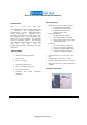
BT111: Bluetooth Smart Ready HCI Module KEY FEATURES DESCRIPTION BT111 is a low cost and ultrasmall Bluetooth Smart Ready HCI module that is designed for applications where both Bluetooth classic and Bluetooth low energy connectivity is needed. BT111 integrates a Bluetooth 4.0 dual mode radio, HCI software stack, USB interface and an antenna.
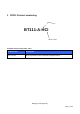
1 BT111 Product numbering Antenna: A = Internal BT111-A-HCI Firmware revision Available products and product codes Product code Description BT111-A-HCI BT111 Bluetooth 4.
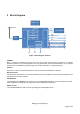
2 Block Diagram 26MHz XTAL Antenna CSR8510 PIO3 RAM 32k EEPROM PIO4 ROM MMU BPF MCU RF LDO 3V3 5V0 3V3 I/O PIO0 PIO1 PIO2 PIO5 3 x LDO 1V3 SPI / PCM LDO 1V8 USB 1V8 Figure 1: Block diagram of BT111 CSR8510 BT111 is based on CSR8510 dual mode chip. The chip includes all the functions required for a complete Bluetooth radio with on chip LDO regulators. The chip provides SPI, PCM and USB interfaces.
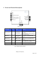
GND USBUSB+ PCM_SYNC/SPI_CS/PIO23 PIO5 PIO2 PCM_CLK/SPI_CLK/PIO24 PCM_IN/SPI_MOSI/PIO21 GND VREG_IN_HV GND VREG_EN_RST# VDD_PADS VREG_OUT_HV VREG_IN_USB VDD_HOST 21 20 19 18 17 16 11 12 13 14 15 1 2 3 4 5 6 7 8 9 10 PIO0 PCM_OUT/SPI_MISO/PIO22 PIO01 SPI_PCM_SEL GND 3 Pinout and Terminal Descriptions Figure 2: BT111 Power Supply Pin No. Pad Type Description Take high to enable internal regulators. Also acts as active low reset.
PIO Port Pin No. PIO0 PIO1 PIO2 PIO5 11 13 6 5 Pad Type Supply Domain Description Bidirectional, tristate, with weak internal pulldown VDD_PADS Programmable input/output line Table 2: I/O Terminal Descriptions PCM Interface Pin No.
4 External Dimensions and Land Pattern Figure 3: Footprint (top view) 7.3mm (+/- 0.1mm) 1.9mm (+/- 10%) 2.1mm (+/- 10%) 13.05mm (+/- 0.1mm) 9.3mm (+/- 0.
5 Layout Guide Lines Use good layout practices to avoid excessive noise coupling to supply voltage traces or sensitive analog signal traces. If using overlapping ground planes use stitching vias separated by max 3 mm to avoid emission from the edges of the PCB. Connect all the GND pins directly to a solid GND plane and make sure that there is a low impedance path for the return current following the signal and supply traces all the way from start to the end.
resonant frequency will be tuned upwards. S11 is a measure of how big portion of the transmitted power is reflected back from the antenna. An adequate performance can be expected if S11 is less than – 7 dB. If using PCB thickness more than 1.6 mm, or if there is dielectric material around the antenna which is likely to detune the resonant frequency, the antenna can be tuned in the mother board layout by removing FR4 below the antenna. Min.
6 Electrical Characteristics 6.1 Absolute Maximum Ratings Rating Min Max Unit Storage temperature -40 +85 -0.2 -0.2 -0.2 -0.2 VSS - 0.4V 5.85 4.9 3.7 3.7 ⁰C V V V V V VREG_IN_USB VREG_IN_HV VDD_HOST VDD_PADS Other terminal voltages VDD + 0.4 V Table 5: Absolute maximum ratings Rating Min Max Unit Operating temperature -30 VREG_IN_USB VREG_IN_HV VDD_HOST 4.25 2.3 3.1 +85 5.75 4.8 3.6 3.6(* ⁰C V V V V VDD_PADS (* 1.7 (* *) NOTE: The internal EEPROM is powered from VDD_PADS.
6.2.2 High-voltage Linear Regulator Normal Operation Min Typ Max Unit Input voltage Output voltage Temperature coefficient Output noise (frequency range 100Hz to 100kHz) Settling time (settling ti within 10% of final value) Output current 2.3 1.75 -200 3.3 1.85 - 4.8 1.95 200 V V ppm/⁰C - - 0.
6.3 Current Consumption Peak (8 dBm) Normal Operation Idle USB Suspend Inguiry File Transfer LE Connected (Master) LE Scan (Master) 73 73 74 48 AVG Unit 5 200 51 58 (* (* mA µA mA mA mA mA *) LE AVG current consumption depends on the chosen TX interval and scanning window Table 10: Current consumption of BT111 with 8 dBm TX power TX Peak = 73 mA Peak = 14 mA 6.5 ms Figure 9: Current consumption profile while creating a SPP connection Peak = 48 mA BGND Current = 6.
Peak = 74 mA AVG = 7.
Figure 13: LE peak current vs.
7 RF Characteristics 7.1 Transmitter Characteristics RF Characetristics, VDD = 3.3V @ room temperature unless otherwise specified Typ Max Bluetooth Specification Unit maximum RF Transmit Power 8 10 20 dBm RF power variation over temperature range 1.5 - dB 0.
Figure 14: Power control steps of BT111 7.2 Receiver Characteristics RF characteristis, VDD = 3.3V, Packet type room temperature Sensitivity for 0.1% BER Sensitivity variation over BT band (* Sensitivity variation over temperature range Min Typ Max Bluetooth Spefication -70 Unit DH1 DH3 DH5 2-DH5 3-DH5 -89 -89 -89 -92 -85 dBm dBm dBm dBm dBm All 2 dB All TBD dB *) Channel 0 @2402Mhz is generally 1.5dB less sensitive than all the other channels.
7.3 Radiated Spurious Emissions Standard FCC part 15 transmitter spurious emissions Min Band / Frequency (AVG / PEAK) 2nd harmonic 3rd harmonic Typ (AVG / PEAK) 51 / 58 < 50 Max (AVG / PEAK) Limit by the Standard (AVG / PEAK) Unit 54 / 74 54 / 74 dBuV/m dBuV/m 54 / 74 dBuV/m 54 / 74 dBuV/m -20 dBc -20 dBc -42 -30 dBm -36 <-40 <-70 <-70 -30 -30 -47 dBm dBm dBm -47 dBm Band edge 2390MHz Band edge 2483.5MHz Band edge 2400MHz (conducted) Band edge 2483.
8 Clock Generation BT111 is using an internal 26 MHz crystal oscillator. All internal digital clocks are generated using a phase locked loop, which is locked to the 26 MHz crystal oscillator. 26 MHz clock is calibrated in production and the calibrated settings are stored to the internal EEPROM of BT111. The 32.768 kHz sleep clock is generated internally to the module. BT111 does not need any external clock sources.
9 Bluetooth Stack Microcontroller BT111 uses a 16-bit RISC MCU for low power consumption and efficient use of memory. The MCU, interrupt controller and event timer run the Bluetooth software stack and control the Bluetooth radio and host interfaces. 10 Programmable I/O Ports See the Device Terminal Functions section for the list of supplies to the PIOs. PIO lines are configured through software to have either weak or strong pull-ups or pull-downs.
12 Memory Management 12.1 Memory Management Unit The MMU provides a number of dynamically allocated ring buffers that hold the data that is in transit between the host and the air. The dynamic allocation of memory ensures efficient use of the available RAM and is performed by a hardware MMU to minimize the overheads on the processor during data/voice transfers. 12.
13 Serial Interfaces 13.1 USB Interface BT111 has a full-speed (12Mbps) USB interface for communicating with other compatible digital devices. The USB interface on BT111 acts as a USB peripheral, responding to requests from a master host controller. BT111 supports the Universal Serial Bus Specification, Revision v2.0 (USB v2.0 Specification) and USB Battery Charging Specification, available from http://www.usb.org.
14 Audio Interfaces BT111 has digital audio interface that is configurable as either a PCM or I2S port. 14.1 PCM Interface The audio PCM interface on the BT111 supports: Continuous transmission and reception of PCM encoded audio data over Bluetooth. Processor overhead reduction through hardware support for continual transmission and reception of PCM data. A bidirectional digital audio interface that routes directly into the baseband layer of the firmware.
PCM_OUT PCM_IN PCM_CLK PCM_SYNC Up to 2400kHz 8/48kHz Figure 16: BT111 as PCM slave 14.1.2 Long Frame Sync Long Frame Sync is the name given to a clocking format that controls the transfer of PCM data words or samples. In Long Frame Sync, the rising edge of PCM_SYNC indicates the start of the PCM word. When BT111 is configured as PCM master, generating PCM_SYNC and PCM_CLK, then PCM_SYNC is 8 bits long. When BT111 is configured as PCM Slave, PCM_SYNC is from 1 cycle PCM_CLK to half the PCM_SYNC rate.
Figure 18: Short Frame Sync (shown with 16-bit sample) As with Long Frame Sync, BT111 samples PCM_IN on the falling edge of PCM_CLK and transmits PCM_OUT on the rising edge. PCM_OUT is configurable as high impedance on the falling edge of PCM_CLK in the LSB position or on the rising edge. 14.2 Multi-slot Operation More than 1 SCO connection over the PCM interface is supported using multiple slots. Up to 3 SCO connections are carried over any of the first 4 slots.
Figure 20: GCI Interface The start of frame is indicated by the rising edge of PCM_SYNC and runs at 8kHz. 14.2.2 Slots and Sample Formats BT111 receives and transmits on any selection of the first 4 slots following each sync pulse. Slot durations are either 8 or 16 clock cycles: 8 clock cycles for 8-bit sample formats. 16 clock cycles for 8-bit, 13-bit or 16-bit sample formats. BT111 supports: 13-bit linear, 16-bit linear and 8-bit μ-law or A-law sample formats. A sample rate of 8ksps.
Figure 21: 16-bit Slot Length and Sample Formats 14.2.3 Additional Features BT111 has a mute facility that forces PCM_OUT to be 0. In master mode, BT111is compatible with some codecs which control power down by forcing PCM_SYNC to 0 while keeping PCM_CLK running.
14.2.4 PCM Timing Information Symbol Parameter 48MHz DDS generation. Frequency selection is programmable. PCM_SYNC frequency for SCO connection fmclkh fmclkl (a) (a) - Typ Max - 128 256 512 - 2.9 - - 8 - - kHz ns 4MHz DDS generation. Ffrequency selection is programmable.
Figure 22: PCM Master Timing Long Frame Sync Figure 23: PCM Master Timing Short Frame Sync Bluegiga Technologies Oy Page 32 of 52
Symbol Parameter fsclkl PCM clock frequency (Slave mode: Input) PCM clock frequency (GCI mode) PCM_CLK low time fsclkh PCM_CLK high time fsclk fsclk Min Typ Max Unit 64 - 2048 kHz 128 200 200 - 4096 - kHz ns ns Table 16: PCM Slave Timing Symbol Parameter Min Typ Max fhsclksynch Hold time from PCM_CLK low to PCM_SYNC high 2 - - fsusclksynch Set-up time for PCM_SYNC high to PCM_CLK low 20 - - fdpout Delay time from PCM_SYNC or PCM_CLK, whichever is later, to valid PCM_OUT d
Figure 25: PCM Slave Timing Short Frame Sync 14.2.5 PCM_CLK and PCM_SYNC Generation BT111 has 2 methods of generating PCM_CLK and PCM_SYNC in master mode: Generating these signals by DDS from BT111 internal 4MHz clock. Using this mode limits PCM_CLK to 128, 256 or 512kHz and PCM_SYNC to 8kHz. Generating these signals by DDS from an internal 48MHz clock, enables a greater range of frequencies to be generated with low jitter but consumes more power.
14.2.6 PCM Configuration Configure the PCM by using PSKEY_PCM_CONFIG32 and PSKEY_PCM_LOW_JITTER_CONFIG, see your PS Key file. The default for PSKEY_PCM_CONFIG32 is 0x00800000, i.e. first slot following sync is active, 13bit linear voice format, long frame sync and interface master generating 256kHz PCM_CLK from 4MHz internal clock with no tri-state of PCM_OUT. 14.3 Digital Audio Interface (I2S) The digital audio interface supports the industry standard formats for I²S, left-justified or right-justified.
Bit Mask Name Description D[0] 0x0001 CONFIG_JUSTIFY_FORMAT D[1] 0x0002 CONFIG_LEFT_JUSTIFY_DELAY D[2] 0x0004 CONFIG_CHANNEL_POLARITY D[3] 0x0008 CONFIG_AUDIO_ATTEN_EN D[7:4] 0x00F0 CONFIG_AUDIO_ATTEN D[9:8] 0x0300 CONFIG_JUSTIFY_RESOLUTION D[10] 0x0400 CONFIG_16_BIT_CROP_EN 0 for left justified, 1 for right justified For left justified formats: 0 is MSB of SD data occurs in the first SCLK period following WS transition. 1 is MSB of SD data occurs in the second SCLK period.
Figure 26: Digital Audio Interface Modes The internal representation of audio samples within BT111 is 16-bit and data on SD_OUT is limited to 16-bit per channel. Symbol Parameter Min Typ Max Unit tch SCK Frequency WS Frequency SCK high time tcl SCK low time 80 80 - 6.
Symbol Parameter WS valid SCK high set-up time SCK high to WS invalid hold time SCK low to SD_OUT valid delay time SD_IN valid to SCK high set-up time SCK high to SD_IN invalid hold time tssu tsh topd tisu tih Min Typ Max Unit 20 - - ns 2.5 - - ns - - 20 ns 20 - - ns 2.5 - - ns 2 Table 21: I C Slave Mode Timing Figure 27: Digital Audio Interface Slave Timing Symbol Parameter - SCK Frequency WS Frequency Min Typ Max Unit - - 6.
Symbol tspd topd tisu tih Parameter SCK low to WS valid delay time SCK low to SD_OUT valid delay time SD_IN valid to SCK high set-up time SCK high to SD_IN invalid hold time Min Typ Max Unit - - 39.27 ns - - 18.44 ns 18.
15 Power Control and Regulation VREG_EN_RST# VBUS (4.25V – 5.75V) LDO 3V3 LDO 1V8 LDO 1V35 LDO 1V35 LDO 1V25 VREG_IN_HV (3.3V OUT / 2.3V – 4.8V IN) VREG_OUT_HV 1.8V OUT / 1.7V – 1.95V IN Figure 29: Internal regulators and powering of BT111 15.1 Voltage Regulator Enable All the regulators are enabled, except the USB linear regulator, by taking the VREG_EN_RST# pin above 1V. Also the BT111 firmware automatically controls the regulators.
15.4 Low Voltage Linear Regulators BT111 has three integrated low voltage linear regulators providing the internal supply voltages for RF and digital circuits of BT111. The input voltage range is between 1.70V and 1.95V. 15.5 Powering Sequence All the power supplies should be powered at the same time. The order of powering the supplies relative to the I/O supply, VDD_PADS to VDD_HOST, is not important.
16 Example Schematic Figure 30: Example schematic for BT111 Bluegiga Technologies Oy Page 42 of 52
17 Software BT111 is supplied with an on-chip Bluetooth v4.0 specification qualified HCI Controller stack firmware. It also has an EEPROM chip, which allows modifications of many configuration parameters (PS-keys) of the Bluetooth chip. When the BT111 development kit is plugged into your PC, it will show up as a generic Bluetooth Controller, and the Bluetooth Host stack installed on your PC will take control of it.
17.1 On-chip Software 17.1.1 Bluetooth HCI Stack Figure 26 shows an example implementation. An internal processor runs the Bluetooth stack up to the HCI. The host processor must provide all the upper layers of Bluetooth protocol including the application.
18 Soldering Recommendations BT111 is compatible with a industrial standard reflow profile for Pb-free solders. The reflow profile used is dependent on the thermal mass of the entire populated PCB, heat transfer efficiency of the oven and particular type of solder paste used. Consult the datasheet of particular solder paste for profile configurations.
19 Certifications 19.1 Bluetooth BT111 is based on Bluetooth v4.0 qualified chip CSR8510 by CSR. BT111 can be used as a controller subsystem with the Bluetooth QD ID B017701. To make a complete Bluetooth end product, Controller Subsystem is used together with a qualified Host Subsystem. 19.2 FCC/IC (USA/Canada) This device complies with Part 15 of the FCC Rules.
IMPORTANT NOTE: In the event that these conditions can not be met (for certain configurations or colocation with another transmitter), then the FCC and Industry Canada authorizations are no longer considered valid and the FCC ID and IC Certification Number can not be used on the final product. In these circumstances, the OEM integrator will be responsible for re-evaluating the end product (including the transmitter) and obtaining a separate FCC and Industry Canada authorization.
Le module transmetteur ne doit pas être installé ou utilisé en concomitance avec une autre antenne ou un autre transmetteur. Tant que ces deux conditions sont réunies, il n’est pas nécessaire de procéder à des tests supplémentaires sur le transmetteur.
19.4 KCC (South-Korea) TBA 19.
20 Moisture Sensitivity Level (MSL) classification Moisture sensitivity level (MSL) of this product is 3. Please follow the handling guidelines of the standard IPC/JEDEC J-STD-020 and J-STD-033.
21 Packaging and Reel Information TBA Bluegiga Technologies Oy Page 51 of 52
22 Contact Information Sales: sales@bluegiga.com Technical support: support@bluegiga.com http://techforum.bluegiga.com Orders: orders@bluegiga.com WWW: www.bluegiga.com www.bluegiga.hk Head Office / Finland: Phone: +358-9-4355 060 Fax: +358-9-4355 0660 Sinikalliontie 5A 02630 ESPOO FINLAND Postal address / Finland: P.O. BOX 120 02631 ESPOO FINLAND Sales Office / USA: Phone: +1 770 291 2181 Fax: +1 770 291 2183 Bluegiga Technologies, Inc.