
User's Manual

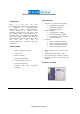


Bluegiga Technologies Oy
Page 10 of 52
PIO Port Pin No. Pad Type Supply Domain Description
PIO0 11
PIO1 13
PIO2 6
PIO5 5
Bidirectional, tristate,
with weak internal pull-
down
VDD_PADS Programmable input/output line
Table 2: I/O Terminal Descriptions
PCM Interface Pin No. Pad Type
Supply
Domain
Description
PCM_OUT/
SPI_MISO/
PIO22
12
Output, tristate, with
weak internal pull-
down
PCM syncronous data output
SPI data output
Programmable input/output line
PCM_IN/
SPI_MOSI/
PIO21
8
Input, tristate, with
weak internal pull-
down
PCM syncronous data input
SPI data input
Programmable input/output line
PCM_SYNC/
SPI_CS#/
PIO23
4
PCM syncronous dara sync
SPI chip select, active low
Programmable input/output line
PCM_CLK/
SPI_CLK/
PIO24
7
PCM syncronous data clock
SPI clock
Pro
g
rammable in
p
ut/out
p
ut line
SPI_PCM#_SEL 14
Input with weak
internal pull-down
High switches SPI/PCM lines to SPI, low
switches SPI/PCM lines to PCM/PIO use
Bidirectional, tristate,
with weak internal
pulldown
VDD_PADS
Table 3: PCM Interface
USB Interface Pin No. Pad Type
Supply
Domain
Description
USB+ 3
USB data plus with selectable internal 1.5k
Ω
pull-up resistor
USB- 2 USB data minus
VDD_HOSTBidirectional
Table 4: USB Interface