
User's Manual


Bluegiga Technologies Oy
Page 9 of 52
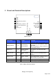
3 Pinout and Terminal Descriptions
1
2
3
4
5
6
7
8
9
10
GND
USB-
USB+
PCM_SYNC/SPI_CS/PIO23
PIO5
PIO2
PCM_CLK/SPI_CLK/PIO24
PCM_IN/SPI_MOSI/PIO21
GND
VREG_IN_HV
11
12
13
14
15
PIO0
PCM_OUT/SPI_MISO/PIO22
PIO01
SPI_PCM_SEL
GND
21
20
19
18
17
16VDD_HOST
VREG_IN_USB
VREG_OUT_HV
VDD_PADS
VREG_EN_RST#
GND
Figure 2: BT111
Power Supply Pin No. Pad Type Description
VREG_EN_RST# 20
Input with strong
internal pull-down
Take high to enable internal regulators. Also
acts as active low reset. Maximum voltage is
VDD_PADS
Note:
USB regulator is always enabled and
not controlled b
y
this
p
in
VREG_IN_HV 10
Analogue regulator
input / output
Input to internal high-voltage regulator to
1.8V regulator, 3.3V output from USB
re
g
ulator.
VREG_OUT_HV 18
Analogue regulator
output
Output from internal high-voltage to 1.8V
regulator. Input to second stage internal
re
g
ulators.
VREG_IN_USB 17
Analogue regulator
input
Input to USB regulator. Connect to external
USB bus supply, e.g. USB_VBUS
VDD_HOST 16 VDD USB system positive supply
VDD_PADS 19 VDD Positive supply for digital I/O pads
Table 1: Supply Terminal Descriptions