
Specifications


AN93
Rev. 0.8 13
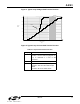
The MINI[1:0] bits select the minimum operational loop
current for the DAA, and the DCV[1:0] bits adjust the
DCT pin voltage, which affects the TIP/RING voltage of
the DAA. These bits allow important trade-offs to be
made between signal headroom and minimum
operational loop current. Increasing TIP/RING voltage
increases signal headroom, whereas decreasing the
TIP/RING voltage allows compliance to PTT standards
in low-voltage countries, such as Japan. Increasing the
minimum operational loop current above 10 mA also
increases signal headroom and prevents degradation of
the signal level in low-voltage countries.
AC Termination
The Si2493/57/34/15/04 has four ac termination
impedances when used with the Si3018 line-side
device. The ACT bits in Register U63 are used to select
the ac impedance setting on the Si3018. The four
available settings for the Si3018 are listed in Table 5. If
an ACT[3:0] setting other than the four listed in Table 5
is selected, the ac termination is forced to 600 Ω
(ACT[3:0] = 0000).
Ringer Impedance and Threshold
The ring detector in many DAAs is ac coupled to the line
with a large 1 µF, 250 V decoupling capacitor. The ring
detector on the Si2493/57/34/15/04 is resistively
coupled to the line. This produces a high ringer
impedance to the line of approximately 20 MΩ to meet
the majority of country PTT specifications, including
FCC and TBR21.
Several countries including Poland, South Africa, and
Slovenia, require a maximum ringer impedance that can
be met with an internally synthesized impedance by
setting the RZ bit (Register 67, bit 1).
Some countries also specify ringer thresholds
differently. The RT bit (Register U67, bit 0) selects
between two different ringer thresholds: 15 V ±10% and
21.5 V ±10%. These two settings satisfy ringer
threshold requirements worldwide. The thresholds are
set so that a ring signal is guaranteed to not be detected
below the minimum, and a ring signal is guaranteed to
be detected above the maximum.
Pulse Dialing and Spark Quenching
Pulse dialing results from going off- and on-hook to
generate make and break pulses. The nominal rate is
10 pulses per second. Some countries have strict
specifications for pulse fidelity that include make and
break times, make resistance, and rise and fall times. In
a traditional solid-state dc holding circuit, there are
many problems in meeting these requirements.
The Si2493/57/34/15/04 dc holding circuit actively
controls the on-hook and off-hook transients to maintain
pulse dialing fidelity.
Spark quenching requirements in countries such as
Italy, the Netherlands, South Africa, and Australia deal
with the on-hook transition during pulse dialing. These
tests provide an inductive dc feed resulting in a large
voltage spike. This spike is caused by the line
inductance and the sudden decrease in current through
the loop when going on-hook. The traditional solution to
the problem is to put a parallel resistive capacitor (RC)
shunt across the hookswitch relay. However, the
capacitor required is large (~1 µF, 250 V) and relatively
expensive. In the Si2493/57/34/15/04, loop current can
be controlled to achieve three distinct on-hook speeds
to pass spark quenching tests without additional BOM
components. Through settings of two bits in two
registers, OHS (Register U67, bit 6) and OHS2
(Register U62, bit 8), a slow ramp down of loop current
can be achieved which induces a delay between the
time the OH bit is cleared and the time the DAA actually
goes on-hook.
Billing Tone Detection
“Billing tones” or “metering pulses” generated by the
central office can cause modem connection difficulties.
The billing tone is typically a 12 kHz or 16 kHz signal
and is sometimes used in Germany, Switzerland, and
South Africa. Depending on line conditions, the billing
tone may be large enough to cause major modem
errors. The Si2493/57/34/15/04 chipset can provide
feedback when a billing tone occurs and when it ends.
Billing tone detection is enabled by setting the BTE bit
(U68, bit 2). Billing tones less than 1.1 V
PK
on the line
are filtered out by the low-pass digital filter on the
Si2493/57/34/15/04. The ROV bit (U68, bit 1) is set
when a line signal is greater than 1.1 V
PK
, indicating a
receive overload condition. The BTD bit is set when a
line signal (billing tone) is large enough to excessively
reduce the line-derived power supply of the line-side
device (Si3018/10). When the BTE bit is set, the dc
termination is changed to an 800 Ω dc impedance. This
ensures minimum line voltage levels even in the
presence of billing tones.
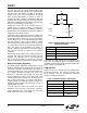
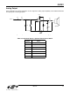
Table 5. AC Termination Settings for the Si3018
Line-Side Device
ACT[3:0] AC Termination
0000 600 Ω
0011 220 Ω + (820 Ω || 120 nF) and 220 Ω +
(820 Ω || 115 nF)
0100 370 Ω + (620 Ω || 310 nF)
1111 Global complex impedance