
Specifications


AN93
Rev. 0.8 155
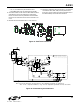
c.C5, C6, C7 IGND return path should be direct.
d.The IGND plane must not extend past Q4 and Q5.
10. The traces from R7 to FB1 and from R8 to FB2 should be
well matched. This can be achieved by routing these
traces next to each other as possible. Ensure that these
traces are not routed close to the traces connected to C1
or C2.
11. Minimize all traces associated with Y1, C26, and C27.
12. Decoupling capacitors (size 0.22 uF and 0.1 uF capacitors
connected to VDA, VDB, VDD) must be placed next to
those pins. Traces of these decoupling capacitors back to
the Si24xx GND pin should be direct and short.
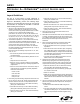
Figure 27. Reference Placement
Figure 28. Illustrated Layout Guidelines+
RING
TIP
4A
4B
4C
4D
4E
4F
4G
4F
5
6
3A
3C 3E
3B
3A
3E
3E
3E3E
7A
7B 7C 7C
7B7B
9A
10
10
11
12
12
12
12
11
8C
8D
8D
9B
9C
9C
9C
11
2
2
22
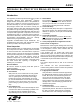
This is not a complete schematic. Only critical component placement and nets are drawn.
1
Traces, pad sites and vias
enclosed in box are in the DAA
section, and must be separated
from all other circuits by 5 mm.
Note: Encircled references are described in the numbered paragraphs in Appendix A.
R9
R8
C9
FB2
C26
RV1
R12
-+
D1
R7
R16
C1
C5
C8
C50
Y1
1 2
U1 Si24HS
XTALI
1
XTALO
2
VDD3.3
5
GND
6
C1A
14
C1B
13
VDDA
7
VDD3.3
21
GND
20
VDDB
19
U2 Si3018
QE
1
DCT
2
RX
3
IB
4
C1B
5
C2B
6
VREG
7
RNG1
8
DCT2
16
IGND
15
DCT3
14
QB
13
QE2
12
SC
11
VREG2
10
RNG2
9
C53
R15
C52
C27
Q5
R2
C2
C7
Q4
+
C4
C6
FB1
C51
R13
C3