
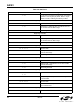
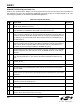
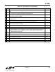
Specifications


AN93
Rev. 0.8 157
16
Distance from TIP and RING through EMC capacitors C8 and C9 to chassis ground is
short.
17
There should be no digital ground plane in the DAA Section.
18
Minimize the area of the loop from U2 pin 7 and pin 10 to C5 and C6 and from those
components to U2 pin 15 (IGND).
19
R2 should be placed next to the base of Q5, and the trace from R2 to U2 pin16 should be
less than 20 mm.
20
Place C4 close to U2 and connect C4 to U2 using a short, direct trace.
21
The area of the loop formed from U2 pin 13 to the base of Q4 and from U2 pin 12 to the
emitter of Q4 should be minimized.
22
The trace from C7 to U2 pin 15 should be short and direct.
23
The trace from C3 to the D1/D2 node should be short and direct.
24
Provide a minimum of 5 mm creepage (or use the capacitor terminal plating spacing as a
guideline for small form factor applications) from any TNV component, pad or trace to
any SELV component, pad or trace.
25
Minimize the area of the loop formed from U2 pin 4 to R9 to U2 pin 15.
26
Cathode marking for Z1.
27
Pin 1 marking for U1 and U2.
28
Space and mounting holes to accommodate for fire enclosure if necessary.
29
IGND plane does not extend under C3, D1, FB1, FB2, R15, R16, C8, C9, or RV1.
Table 101. Layout Check List (Continued)
3 #Layout Items Required