
Specifications


AN93
Rev. 0.9 59
A CRC can be run on the upgrade file loaded into on-
chip Program RAM with the AT&T6 command to verify
that the upgrade was correctly written to the on-chip
memory. The CRC value obtained from executing the
AT&T6 command should match the CRC value provided
with the upgrade code.
The following memory notation conventions are
followed in this document:
Single variable U-Registers are identified in this
document as the register type (i.e., U) followed by
the last two digits of the register’s hexadecimal
address and finally the register “name” in
parenthesis. Example: U4A(RGFD). Once the full
register reference is made, continuing discussion
refers to the register name to simplify the text. The
address and value of a single variable U-Register
are always read from or written to the Si2493/57/34/
15/04 in hexadecimal.
Bit-mapped U-Registers are identified in this
document at the top level as the register type (i.e.,
U) followed by the last two digits of the register’s
hexadecimal address and finally the register “name”
in parenthesis. Example: U67 (ITC1). Once the full
register reference is made, continuing discussion of
the register at the top level refers to the register
name to simplify the text. The address and value of a
bit-mapped U-Register is always read from or written
to the Si2493/57/34/15/04 in hexadecimal.
Bits within bit-mapped registers are identified in this
document as the register type (i.e., U) followed by
the last two digits of the register’s hexadecimal
address, the bit or bit range within the register in
brackets, and finally the bit or bit range “name” in
parenthesis. Example: U67[6](OHS) or
U67[3:2](DCT). Once the full register reference is
made, continuing discussion of the bits or bit range
refers to the bit or bit range name to simplify the text.
The bit or bit range inside the bracket represents the
actual bit or bit range within the register. The value of
a bit or bit range is presented in binary for clarity.
However, the address and value of a bit-mapped U-
Register is always read from or written to the Si2493/
57/34/15/04 in hexadecimal.
Si2493/57/34/15/04 S-Registers are identified with a
decimal address (e.g., S38), and the number stored
in an S-Register is also a decimal value.
3.3.2. EEPROM Interface
(24-Pin TSSOP Only)
The ISOmodem chipset supports an optional serial
peripheral interface (SPI) bus EEPROM. The EEPROM
must support SPI mode 3 with a 16-bit (8 kbit – 64 kbit
range) address. Upon powerup, if a pulldown resistor
<
10 kΩ is placed between D6 (Si2493/57/34/15/04, pin
4) and GND, the Si2493/57/34/15/04 attempts to detect
an EEPROM. The modem looks for a carriage return in
the first 10 memory locations. If none is found
(unprogrammed EEPROM), the modem stops reading
the EEPROM. An installed EEPROM may contain
custom default settings, firmware upgrades, and/or
user-defined AT command macros for use in custom AT
commands or country codes.
Once the EEPROM is detected, customer defaults that
are programmed into the EEPROM between the
optional heading "BOOT" and the "<CR><CR>"
delimiter execute immediately, and AT command
macros are loaded into on-chip RAM. The memory that
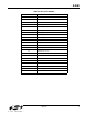
Table 25. Load Technique and Speed Table*
Start Condition: Delay
between lines
Load Time (sec)
for a 6235 byte patch
(at 115 kBaud)
Approach used with:
RESET then
ATE0 & ATQ1
0.5 ms 0.694 Embedded Systems
1.0 ms 0.771 Embedded Systems
2.0 ms 0.925 Embedded Systems
5.0 ms 1.385 Embedded Systems
10.0 ms 2.152 Embedded Systems
RESET Wait for OK/
CR/LF
3.998 Windows or Embedded System where
time precision is poorer than 10 ms
RESET 100.0 ms 15.962 Windows without writing a patch loader
*Note: The delay times do not include the time to empty the UART's possibly long TX buffer. The time quoted is between the
end of transmission of the last character of a line and the start of transmission of the first character of the next line.