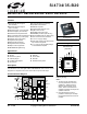
Si4734/35-B20 B ROADCAST AM/FM/SW/LW R ADIO R ECEIVER Features Worldwide FM band support (64–108 MHz) Worldwide AM band support (520–1710 kHz) SW band support (2.3–21.
Si4734/35-B20 2 Rev. 1.
Si4734/35-B20 TABLE O F C ONTENTS Section Page 1. Electrical Specifications . . . . . . . . . . . . . . . . . . . . . . . . . . . . . . . . . . . . . . . . . . . . . . . . . . .4 2. Typical Application Schematic . . . . . . . . . . . . . . . . . . . . . . . . . . . . . . . . . . . . . . . . . . . . . 17 3. Bill of Materials . . . . . . . . . . . . . . . . . . . . . . . . . . . . . . . . . . . . . . . . . . . . . . . . . . . . . . . . . . 18 4. Functional Description . . . . . . . . . . . . . . . . . . . .
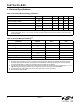
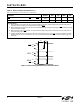
Si4734/35-B20 1. Electrical Specifications Table 1. Recommended Operating Conditions Parameter Symbol Test Condition Min Typ Max Unit Supply Voltage VDD 2.7 — 5.5 V Interface Supply Voltage VIO 1.5 — 3.6 V Power Supply Powerup Rise Time VDDRISE 10 — — µs Interface Power Supply Powerup Rise Time VIORISE 10 — — µs TA –20 25 85 °C Ambient Temperature Note: All minimum and maximum specifications are guaranteed and apply across the recommended operating conditions.
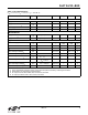
Si4734/35-B20 Table 3. DC Characteristics (VDD = 2.7 to 5.5 V, VIO = 1.5 to 3.6 V, TA = –20 to 85 °C) Parameter Symbol Test Condition Min Typ Max Unit — 19.2 22 mA — 19.8 23 mA — 19.9 23 mA FM Mode Supply Current Supply Current IFM 1 IFM RDS Supply Current2 Supply Current Low SNR level IFM 2 IFMD Digital Output Mode — 18.0 20.5 mA Supply Current IAM Analog Output Mode — 17.3 20.5 mA Supply Current2 IAMD Digital Output Mode — 15.5 20.
Si4734/35-B20 Table 4. Reset Timing Characteristics1,2,3 (VDD = 2.7 to 5.5 V, VIO = 1.5 to 3.6 V, TA = –20 to 85 °C) Parameter Symbol Min Typ Max Unit RST Pulse Width and GPO1, GPO2/INT Setup to RST↑4 tSRST 100 — — µs GPO1, GPO2/INT Hold from RST↑ tHRST 30 — — ns Important Notes: 1. When selecting 2-wire mode, the user must ensure that a 2-wire start condition (falling edge of SDIO while SCLK is high) does not occur within 300 ns before the rising edge of RST. 2.
Si4734/35-B20 Table 5. 2-Wire Control Interface Characteristics1,2,3 (VDD = 2.7 to 5.5 V, VIO = 1.5 to 3.6 V, TA = –20 to 85 °C) Parameter Symbol Test Condition Min Typ Max Unit SCLK Frequency fSCL 0 — 400 kHz SCLK Low Time tLOW 1.3 — — µs SCLK High Time tHIGH 0.6 — — µs SCLK Input to SDIO ↓ Setup (START) tSU:STA 0.6 — — µs SCLK Input to SDIO ↓ Hold (START) tHD:STA 0.
Si4734/35-B20 SCLK SDIO tSU:STA tHD:STA tLOW START tr:IN tHIGH tr:IN tf:IN tSP tSU:STO tBUF 70% 30% 70% 30% tf:IN, tf:OUT tHD:DAT tSU:DAT STOP START Figure 2. 2-Wire Control Interface Read and Write Timing Parameters SCLK A6-A0, R/W SDIO START ADDRESS + R/W D7-D0 ACK DATA D7-D0 ACK DATA ACK Figure 3. 2-Wire Control Interface Read and Write Timing Diagram 8 Rev. 1.
Si4734/35-B20 Table 6. 3-Wire Control Interface Characteristics (VDD = 2.7 to 5.5 V, VIO = 1.5 to 3.6 V, TA = –20 to 85 °C) Parameter Symbol Test Condition Min Typ Max Unit SCLK Frequency fCLK 0 — 2.
Si4734/35-B20 Table 7. SPI Control Interface Characteristics (VDD = 2.7 to 5.5 V, VIO = 1.5 to 3.6 V, TA = –20 to 85 °C) Parameter Symbol Test Condition Min Typ Max Unit SCLK Frequency fCLK 0 — 2.
Si4734/35-B20 Table 8. Digital Audio Interface Characteristics (VDD = 2.7 to 5.5 V, VIO = 1.5 to 3.
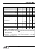
Si4734/35-B20 Table 9. FM Receiver Characteristics1,2 (VDD = 2.7 to 5.5 V, VIO = 1.5 to 3.6 V, TA = –20 to 85 °C) Parameter Symbol Input Frequency Test Condition fRF Min Typ Max Unit 76 — 108 MHz Sensitivity with Headphone Network3,4,5 (S+N)/N = 26 dB — 2.2 3.5 µV EMF Sensitivity with 50 Ω Network3,4,5,6 (S+N)/N = 26 dB — 1.1 — µV EMF RDS Sensitivity6 Δf = 2 kHz, RDS BLER < 5% — 15 — µV EMF 3 4 5 kΩ 4 5 6 pF 100 105 — dBµV EMF m = 0.
Si4734/35-B20 Table 9. FM Receiver Characteristics1,2 (Continued) (VDD = 2.7 to 5.5 V, VIO = 1.5 to 3.6 V, TA = –20 to 85 °C) Parameter Symbol Seek/Tune Time6 Powerup Time6 12 RSSI Offset Test Condition Min Typ Max Unit RCLK tolerance = 100 ppm — — 80 ms/channel From powerdown — — 110 ms Input levels of 8 and 60 dBµV at RF Input –3 — 3 dB Notes: 1. Additional testing information is available in Application Note AN388. Volume = maximum for all tests. Tested at RF = 98.1 MHz. 2.
Si4734/35-B20 Table 10. 64–75.9 MHz Input Frequency FM Receiver Characteristics1 (VDD = 2.7 to 5.5 V, VIO = 1.5 to 3.6 V, TA = –20 to 85 °C) Parameter Symbol Min Typ Max Unit 64 — 75.9 MHz — 4.0 — µV EMF LNA Input Resistance5,6 3 4 5 kΩ LNA Input Capacitance5,6 4 5 6 pF 100 105 — dBµV EMF m = 0.
Si4734/35-B20 Table 11. AM/SW/LW Receiver Characteristics1 (VDD = 2.7 to 5.5 V, VIO = 1.5 to 3.6 V, TA = –20 to 85 °C) Parameter Input Frequency Sensitivity 2,3,4,5, 6 Large Signal Voltage Handling5,7 Power Supply Rejection Ratio Symbol fRF Test Condition Min Typ Max Unit Long Wave (LW) 153 — 279 kHz Medium Wave (AM) 520 — 1710 kHz Short Wave (SW) 2.3 — 21.
Si4734/35-B20 Table 12. Reference Clock and Crystal Characteristics (VDD = 2.7 to 5.5 V, VIO = 1.5 to 3.6 V, TA = –20 to 85 °C) Parameter Symbol Test Condition Min Typ Max Unit 31.130 32.768 40000.0 kHz –50 — 50 ppm 1 — 4095 31.130 32.768 34.406 kHz Crystal Oscillator Frequency — 32.768 — kHz Crystal Frequency Tolerance* –100 — 100 ppm — — 3.
Si4734/35-B20 2. Typical Application Schematic GPO1 GPO2/INT L1 16 DFS 17 GPO3 18 GPO2 19 DFS DOUT 15 R3 DOUT Optional: Digital Audio Output LOUT 14 ROUT 13 GND 12 LOUT ROUT VBATTERY 2.7 to 5.5 V 10 7 VIO C1 6 RST DCLK VDD 11 AMI RST RCLK 5 9 4 SEN C5 SDIO L2 U1 Si4734/35-GM 8 C4 SCLK FMI 1 NC 2 FMI 3 RFGND GPO1 NC 20 R1 R2 X1 GPO3 SEN SCLK C2 SDIO RCLK VIO 1.5 to 3.6 V RCLK C3 Optional: for crystal oscillator option Notes: 1. Place C1 close to VDD pin. 2.
Si4734/35-B20 3. Bill of Materials Component(s) Value/Description Supplier C1 Supply bypass capacitor, 22 nF, ±20%, Z5U/X7R Murata C4 Capacitor, 18 pF, ±20%, Z5U/X7R Murata C5 Coupling capacitor, 0.47 µF, ±20%, Z5U/X7R Murata L1 Ferrite loop stick, 180–450 µH Jiaxin L2 4.7 µH U1 Si4734/35 AM/FM Radio Tuner Coilcraft Silicon Laboratories Optional Components C2, C3 X1 R1, R2 R3 18 Crystal load capacitors, 22 pF, ±5%, COG (Optional: for crystal oscillator option) Venkel 32.
Si4734/35-B20 4. Functional Description 4.1. Overview FM / SW ANT Si4734/35 FMI RDS (Si4735) AGC LOW-IF ADC AMI LNA ADC DFS GPO/DCLK ROUT DAC LOUT AFC RCLK LDO CONTROL INTERFACE VIO 1.5-3.6V RST VDD GND DOUT DAC SDIO AGC 2.7 - 5.5 V DIGITAL AUDIO (Si4735) DSP SCLK RFGND SEN AM / LW ANT LNA Figure 9. Functional Block Diagram The Si4734/35 is the industry's first fully integrated, 100% CMOS AM/FM/SW/LW radio receiver IC.
Si4734/35-B20 4.2. Operating Modes The Si4734/35 operates in either an FM receive or an AM/SW/LW receive mode. In FM mode, radio signals are received on FMI (pin 2) and processed by the FM front-end circuitry. In AM/SW/LW mode, radio signals are received on AMI (pin 4) and processed by the AM front-end circuitry. In addition to the receiver mode, a clocking mode allows the Si4734/35 to be clocked from a reference clock or crystal.
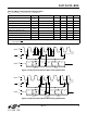
Si4734/35-B20 4.7. Digital Audio Interface (Si4735 Only) The digital audio interface operates in slave mode and supports three different audio data formats: I2S Left-Justified DSP Mode 4.7.1. Audio Data Formats In I2S mode, by default the MSB is captured on the second rising edge of DCLK following each DFS transition. The remaining bits of the word are sent in order, down to the LSB. The left channel is transferred first when the DFS is low, and the right channel is transferred when the DFS is high.
Si4734/35-B20 (OFALL = 1) INVERTED DCLK (OFALL = 0) DCLK LEFT CHANNEL DFS I2S (OMODE = 0000) RIGHT CHANNEL 1 DCLK 1 DCLK 1 DOUT 2 n-2 3 n-1 MSB n 1 LSB MSB 2 n-2 3 n-1 n LSB Figure 10. I2S Digital Audio Format (OFALL = 1) INVERTED DCLK (OFALL = 0) DCLK DFS LEFT CHANNEL RIGHT CHANNEL Left-Justified (OMODE = 0110) 1 DOUT 2 3 n-2 n-1 MSB n 1 LSB MSB 2 n-2 3 n-1 n LSB Figure 11.
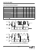
Si4734/35-B20 4.9. De-emphasis The output of the FM demodulator is a stereo multiplexed (MPX) signal. The MPX standard was developed in 1961, and is used worldwide. Today's MPX signal format consists of left + right (L+R) audio, left – right (L–R) audio, a 19 kHz pilot tone, and RDS/RBDS data as shown in Figure 13. Pre-emphasis and de-emphasis is a technique used by FM broadcasters to improve the signal-to-noise ratio of FM receivers by reducing the effects of high-frequency interference and noise.
Si4734/35-B20 4.13. Tuning The frequency synthesizer uses Silicon Laboratories’ proven technology, including a completely integrated VCO. The frequency synthesizer generates the quadrature local oscillator signal used to downconvert the RF input to a low intermediate frequency. The VCO frequency is locked to the reference clock and adjusted with an automatic frequency control (AFC) servo loop during reception. The tuning frequency can be directly programmed using the FM_TUNE_FREQ and AM_TUNE_FREQ commands.
Si4734/35-B20 word by driving SDIO low on the next falling edge of SCLK. Although the Si4734/35 will respond to only a single device address, this address can be changed with the SEN pin (note that the SEN pin is not used for signaling in 2-wire mode). When SEN = 0, the 7-bit device address is 0010001b. When SEN = 1, the address is 1100011b. For write operations, the user then sends an 8-bit data byte on SDIO, which is captured by the device on rising edges of SCLK.
Si4734/35-B20 will be ignored by the device if the transaction is aborted. For details on timing specifications and diagrams, refer to Figure 6 and Figure 7 on page 10. 4.17. GPO Outputs The Si4734/35 provides five general-purpose output pins. The GPO pins can be configured to output a constant low, constant high, or high-impedance. The GPO pins can be reconfigured as specialized functions.
Si4734/35-B20 5. Commands and Properties Table 14. Si473x Command Summary Cmd Name Description 0x01 POWER_UP 0x10 GET_REV 0x11 POWER_DOWN Power down device. 0x12 SET_PROPERTY Sets the value of a property. 0x13 GET_PROPERTY Retrieves a property’s value. 0x14 GET_INT_STATUS Read interrupt status bits. 0x15 PATCH_ARGS Reserved command used for firmware file downloads. 0x16 PATCH_DATA Reserved command used for firmware file downloads. 0x20 FM_TUNE_FREQ Selects the FM tuning frequency.
Si4734/35-B20 Table 15. Si473x Property Summary Prop Name 0x0001 GPO_IEN Description Enables interrupt sources. 0x0102 DIGITAL_OUTPUT_FORMAT Configures the digital output format (Si4735 only). Default 0x0000 0x0000 0x0104 DIGITAL_OUTPUT_ SAMPLE_RATE Configures the digital output sample rate in 100 Hz steps. The digital output sample rate is disabled by default (Si4735 only). 0x0000 0x0201 REFCLK_FREQ Sets frequency of reference clock in Hz.
Si4734/35-B20 Table 15. Si473x Property Summary (Continued) Prop Name Description Default 0x1502 RDS_CONFIG 0x3100 AM_DEEMPHASIS 0x3102 AM_CHANNEL_FILTER Selects the bandwidth of the channel filter for AM/SW/LW reception. The choices are 6, 4, 3, 2, or 1 (kHz). The default band0x0003 width is 2 kHz. 0x3200 AM_RSQ_INTERRUPTS Configures interrupt related to RSQ metrics. All interrupts are disabled by default. 0x0000 0x3201 AM_RSQ_SNR_HIGH_ THRESHOLD Sets high threshold for SNR interrupt.
Si4734/35-B20 GPO2/INT GPO3/DCLK DFS 1 GPO1 NC NC 6. Pin Descriptions: Si4734/35-GM 20 19 18 17 16 FMI 2 15 DOUT RFGND 3 14 LOUT GND PAD AMI 4 13 ROUT 6 7 8 9 10 SCLK SDIO RCLK VIO 12 GND SEN RST 5 11 VDD Pin Number(s) Name 1, 20 NC No connect. Leave floating. 2 FMI FM RF inputs. 3 RFGND 4 AMI AM/SW/LW RF input. 5 RST Device reset (active low) input. 6 SEN Serial enable input (active low). 7 SCLK Serial clock input. 8 SDIO Serial data input/output.
Si4734/35-B20 7. Ordering Guide Part Number* Description Package Type Operating Temperature Si4734-B20-GM AM/FM/SW/LW Broadcast Radio Receiver QFN Pb-free –20 to 85 °C Si4735-B20-GM AM/FM/SW/LW Broadcast Radio Receiver with RDS/RBDS QFN Pb-free –20 to 85 °C *Note: Add an “(R)” at the end of the device part number to denote tape and reel option; 2500 quantity per reel. Rev. 1.
Si4734/35-B20 8. Package Markings (Top Marks) 8.1. Si4734/35 Top Mark 3420 BTTT YWW 3520 BTTT YWW 8.2. Top Mark Explanation Mark Method: YAG Laser Line 1 Marking: Part Number 34 = Si4734, 35 = Si4735 Firmware Revision 20 = Firmware Revision 2.0 Die Revision B = Revision B Die TTT = Internal Code Internal tracking code. Line 2 Marking: Line 3 Marking: Circle = 0.5 mm Diameter Pin 1 Identifier (Bottom-Left Justified) Y = Year WW = Workweek 32 Assigned by the Assembly House.
Si4734/35-B20 9. Package Outline: Si4734/35 QFN Figure 14 illustrates the package details for the Si4734/35. Table 16 lists the values for the dimensions shown in the illustration. Figure 14. 20-Pin Quad Flat No-Lead (QFN) Table 16. Package Dimensions Symbol Millimeters Symbol Millimeters Min Nom Max A 0.50 0.55 0.60 f A1 0.00 0.02 0.05 L 0.35 0.40 0.45 b 0.20 0.25 0.30 L1 0.00 — 0.10 c 0.27 0.32 0.37 aaa — — 0.05 bbb — — 0.05 ccc — — 0.08 ddd — — 0.
Si4734/35-B20 10. PCB Land Pattern: Si4734/35 QFN Figure 15 illustrates the PCB land pattern details for the Si4734/35-GM. Table 17 lists the values for the dimensions shown in the illustration. Figure 15. PCB Land Pattern 34 Rev. 1.
Si4734/35-B20 Table 17. PCB Land Pattern Dimensions Symbol Millimeters Min D D2 Symbol Max 2.71 REF 1.60 1.80 Min Max GE 2.10 — W — 0.34 — e 0.50 BSC X E 2.71 REF Y E2 f GD 1.60 1.80 2.53 BSC 2.10 Millimeters 0.28 0.61 REF ZE — 3.31 ZD — 3.31 — Notes: General 1. All dimensions shown are in millimeters (mm) unless otherwise noted. 2. Dimensioning and Tolerancing is per the ANSI Y14.5M-1994 specification. 3. This Land Pattern Design is based on IPC-SM-782 guidelines. 4.
Si4734/35-B20 11. Additional Reference Resources 36 EN55020 Compliance Test Certificate AN231: Si4700/01 Headphone and Antenna Interface AN332: Universal Programming Guide AN383: Antenna Selection and Universal Layout Guidelines AN386: Si473x Ferrite Loop Stick Antenna Interface AN388: Universal Evaluation Board Test Procedure AN389: Si473x EVB Quick-Start Guide Si47xx Customer Support Site: http://www.mysilabs.
Si4734/35-B20 DOCUMENT CHANGE LIST Revision 0.4 to Revision 1.0 Updated Table 1, “Recommended Operating Conditions,” on page 4. Updated Table 3, “DC Characteristics,” on page 5. Updated Table 5, “2-Wire Control Interface Characteristics1,2,3,” on page 7. Updated Table 8, “Digital Audio Interface Characteristics,” on page 11. Updated Table 9, “FM Receiver Characteristics1,2,” on page 12. Updated Table 10, “64–75.9 MHz Input Frequency FM Receiver Characteristics1,” on page 14.
Si4734/35-B20 CONTACT INFORMATION Silicon Laboratories Inc. 400 West Cesar Chavez Austin, TX 78701 Tel: 1+(512) 416-8500 Fax: 1+(512) 416-9669 Toll Free: 1+(877) 444-3032 Email: FMinfo@silabs.com Internet: www.silabs.com The information in this document is believed to be accurate in all respects at the time of publication but is subject to change without notice.