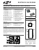
Si4730/31/34/35-D60 B ROADCAST AM/FM/SW/LW R ADIO R ECEIVER Features Ordering Information: See page 33.
Si4730/31/34/35-D60 2 Rev. 1.
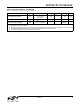
Si4730/31/34/35-D60 TABLE O F C ONTENTS Section Page 1. Electrical Specifications . . . . . . . . . . . . . . . . . . . . . . . . . . . . . . . . . . . . . . . . . . . . . . . . . . .5 2. Typical Application Schematic . . . . . . . . . . . . . . . . . . . . . . . . . . . . . . . . . . . . . . . . . . . . . 20 2.1. QFN Typical Application Schematic . . . . . . . . . . . . . . . . . . . . . . . . . . . . . . . . . . . . . 20 2.2. SSOP Typical Application Schematic . . . . . . . . . . . . . . . . . . . . . .
Si4730/31/34/35-D60 8.1. Si473x-D60 QFN . . . . . . . . . . . . . . . . . . . . . . . . . . . . . . . . . . . . . . . . . . . . . . . . . . . . 36 8.2. Si473x-D60 SSOP . . . . . . . . . . . . . . . . . . . . . . . . . . . . . . . . . . . . . . . . . . . . . . . . . . 38 9. Top Markings . . . . . . . . . . . . . . . . . . . . . . . . . . . . . . . . . . . . . . . . . . . . . . . . . . . . . . . . . . .39 9.1. Si473x-D60 Top Marking (QFN) . . . . . . . . . . . . . . . . . . . . . . . . . . . . . . . . . . . .
Si4730/31/34/35-D60 1. Electrical Specifications Table 1. Recommended Operating Conditions1 Parameter Symbol Test Condition Min Typ Max Unit Analog Supply Voltage VA 2.72 — 5.5 V Digital and I/O Supply Voltage VD 1.62 — 3.6 V Power Supply Powerup Rise Time VDDRISE 10 — — µs Interface Power Supply Powerup Rise Time VIORISE 10 — — µs TA –20 25 85 C Ambient Temperature Notes: 1. All minimum and maximum specifications apply across the recommended operating conditions.
Si4730/31/34/35-D60 Table 2. DC Characteristics (VA = 2.7 to 5.5 V, VD = 1.62 to 3.6 V, TA = –20 to 85 °C) Parameter Symbol Test Condition Min Typ Max — 8.2 9.5 — 10.5 13.5 — 18.5 21.5 Unit FM Mode VAQFN Supply Current IFMVA VDQFN Supply Current IFMVD VASSOP Supply Current IFMVA VDSSOP Supply Current IFMVD — 0.15 0.6 VAQFN Supply Current IFMVA — 9.1 10.3 VDQFN Supply Current IFMVD — 9.9 12.8 VASSOP Supply Current IFMVA — 19.1 21.3 VDSSOP Supply Current IFMVD 0.
Si4730/31/34/35-D60 Table 2. DC Characteristics (Continued) (VA = 2.7 to 5.5 V, VD = 1.62 to 3.6 V, TA = –20 to 85 °C) Parameter Symbol Test Condition Min Typ Max Unit IIL VIN = 0 V, VD = 3.6 V –10 — 10 µA High Level Output Voltage4 VOH IOUT = 500 µA 0.8 x VD — — V Low Level Output Voltage4 VOL IOUT = –500 µA — — 0.2 x VD V 3 Low Level Input Current Notes: 1. Guaranteed by characterization. 2. Backwards compatible mode to rev B and rev C.
Si4730/31/34/35-D60 Table 3. Reset Timing Characteristics1,2,3 (VA = 2.7 to 5.5 V, VD = 1.62 to 3.6 V, TA = –20 to 85 °C) Parameter Symbol Min Typ Max Unit RST Pulse Width and GPO1, GPO2/INT Setup to RST tSRST 100 — — µs GPO1, GPO2/INT Hold from RST tHRST 30 — — ns Important Notes: 1. When selecting 2-wire mode, the user must ensure that a 2-wire start condition (falling edge of SDIO while SCLK is high) does not occur within 300 ns before the rising edge of RST. 2.
Si4730/31/34/35-D60 Table 4. 2-Wire Control Interface Characteristics1,2,3 (VA = 2.7 to 5.5 V, VD = 1.62 to 3.6 V, TA = –20 to 85 °C) Parameter Symbol Test Condition Min Typ Max Unit SCLK Frequency fSCL 0 — 400 kHz SCLK Low Time tLOW 1.3 — — µs SCLK High Time tHIGH 0.6 — — µs SCLK Input to SDIO Setup (START) tSU:STA 0.6 — — µs SCLK Input to SDIO Hold (START) tHD:STA 0.
Si4730/31/34/35-D60 SCLK SDIO tSU:STA tHD:STA tLOW START tr:IN tHIGH tr:IN tf:IN tSP tSU:STO tBUF 70% 30% 70% 30% tf:IN, tf:OUT tHD:DAT tSU:DAT STOP START Figure 2. 2-Wire Control Interface Read and Write Timing Parameters SCLK A6-A0, R/W SDIO START ADDRESS + R/W D7-D0 ACK DATA D7-D0 ACK DATA ACK Figure 3. 2-Wire Control Interface Read and Write Timing Diagram 10 Rev. 1.
Si4730/31/34/35-D60 Table 5. 3-Wire Control Interface Characteristics (VA = 2.7 to 5.5 V, VD = 1.62 to 3.6 V, TA = –20 to 85 °C) Parameter Symbol Test Condition Min Typ Max Unit SCLK Frequency fCLK 0 — 2.
Si4730/31/34/35-D60 Table 6. Digital Audio Interface Characteristics (VA = 2.7 to 5.5 V, VD = 1.62 to 3.
Si4730/31/34/35-D60 Table 7. FM Receiver Characteristics1,2 (VA = 2.7 to 5.5 V, VD = 1.62 to 3.6 V, TA = –20 to 85 °C) Parameter Symbol Min Typ Max Unit 76 — 108 MHz (S+N)/N = 26 dB — 2.2 3.5 µV EMF f = 2 kHz, RDS BLER < 5% — 10 — µV EMF 3 4 5 k 4 5 6 pF 100 105 — dBµV EMF m = 0.
Si4730/31/34/35-D60 Table 7. FM Receiver Characteristics1,2 (Continued) (VA = 2.7 to 5.5 V, VD = 1.62 to 3.
Si4730/31/34/35-D60 Table 8. 64–75.9 MHz Input Frequency FM Receiver Characteristics1,2,3 (VA = 2.7 to 5.5 V, VD = 1.62 to 3.6 V, TA = –20 to 85 °C) Parameter Symbol Min Typ Max Unit 64 — 75.9 MHz — 3.5 — µV EMF 3 4 5 k 4 5 6 pF — 105 — dBµV EMF m = 0.
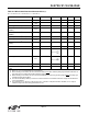
Si4730/31/34/35-D60 Table 9. AM/SW/LW Receiver Characteristics1,2 (VA = 2.7 to 5.5 V, VA = 1.62 to 3.6 V, TA = –20 to 85 °C) Parameter Symbol Test Condition Min Typ Max Unit fRF Long Wave (LW) 153 — 279 kHz Medium Wave (AM) 520 — 1710 kHz Short Wave (SW) 2.3 — 26.1 MHz (S+N)/N = 26 dB — 25 35 µV EMF THD < 8% — 300 — mVRMS ∆VDD = 100 mVRMS, 100 Hz — 40 — dB Audio Output Voltage3,7 54 60 67 mVRMS 3,4,7 — 60 — dB — 0.1 0.
Si4730/31/34/35-D60 Table 10. AC Receiver Characteristics—AUXIN Analog to Digital Converter (VA = 2.7 to 5.5 V, VD = 1.62 to 3.6 V, TA = –20 to 85 °C) Parameter Symbol Test Condition Min Typ Max Unit THD+N f = 1 kHz; measured 20 Hz—20 kHz — 0.035 0.06 % SNR f = 1 kHz at –60 dBFS A-weighted — 85 — dB f = 1 kHz at –60 dBFS non-weighted — 78 — dB f = 1 kHz with 3% Bandpass filter — 90 — dB Gain Mismatch — 0.
Si4730/31/34/35-D60 Table 12. Reference Clock and Crystal Characteristics (VA = 2.7 to 5.5 V, VD = 1.62 to 3.6 V, TA = –20 to 85 °C) Parameter Symbol Test Condition Min Typ Max Unit 31.130 32.768 40,000 kHz –100 — 100 ppm 1 — 4095 31.130 32.768 34.406 kHz — 32.768 — kHz –100 — 100 ppm Board Capacitance — — 3.
Si4730/31/34/35-D60 Table 14. Absolute Maximum Ratings1,2 Parameter Symbol Value Unit Analog Supply Voltage VA –0.5 to 5.8 V Digital and I/O Supply Voltage VD –0.5 to 3.9 V Input Current3 IIN 10 mA 3 VIN –0.3 to (VIO + 0.3) V Operating Temperature TOP –40 to 95 C Storage Temperature TSTG –55 to 150 C 0.4 Vpk Input Voltage RF Input Level4 Notes: 1. Permanent device damage may occur if the above Absolute Maximum Ratings are exceeded.
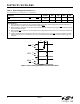
Si4730/31/34/35-D60 2. Typical Application Schematic 2.1. QFN Typical Application Schematic DFS DOUT GP03/DCLK LOUT ROUT 16 C7 15 C8 Optional: Digital Audio Out RIN OPMODE: 0xB0, 0xB5 LIN 17 R3 14 R2 13 R1 DCLK C9 GPO1 DFS GPO2/INT DOUT R3 Si473x GPO3/DCLK R2 16 17 DOUT DFS 19 18 GPO3/DCLK LOUT ROUT Si473x GND RSTB VA 15 14 LOUT 13 ROUT 12 2.7 to 5.
Si4730/31/34/35-D60 2.2.
Si4730/31/34/35-D60 3. Bill of Materials 3.1. QFN/SSOP Bill of Materials Table 15. Si473x-D60 QFN/SSOP Bill of Materials Component(s) Value/Description Supplier C1 Supply bypass capacitor, 22 nF, ±20%, Z5U/X7R Murata C2 Coupling capacitor, 1 nF, ±20%, Z5U/X7R Murata C3 Coupling capacitor, 0.
Si4730/31/34/35-D60 4. Functional Description 4.1. Overview Si473x-D60 RIN LIN RDS (Si4731/ 35) FMI LNA AMI AGC 2.7~5.5 V ROUT DAC LOUT CONTROL INTERFACE AFC SEN RCLK LDO DAC DSP ADC Mux VA GND GPO/DCLK ADC Mux LNA DFS VD 1.62~3.6 V RST RFGND DIGITAL AUDIO SDIO AM / LW ANT DOUT LOW-IF AGC SCLK FM / SW ANT Figure 7.
Si4730/31/34/35-D60 4.2. Operating Modes The Si473x-D60 operates in either an FM receive, AM receive, or audio AUXIN ADC mode. In FM mode, radio signals are received on FMI and processed by the FM front-end circuitry. In AM mode, radio signals are received on AMI and processed by the AM front-end circuitry. In audio AUXIN ADC mode, stereo audio signals on LIN/RIN are sampled, converted to digital, filtered, and decimated to 32, 44.1, or 48 kHz for the I2S digital audio interface.
Si4730/31/34/35-D60 4.8. Digital Audio Interface The digital audio interface operates in slave mode and supports a variety of MSB-first audio data formats including I2S and left-justified modes. The interface has three pins: digital data input (DIN), digital frame synchronization input (DFS), and a digital bit synchronization input clock (DCLK). The Si473x-D60 supports a number of industry-standard sampling rates including 32, 44.1, and 48 kHz.
Si4730/31/34/35-D60 (OFALL = 1) INVERTED DCLK (OFALL = 0) DCLK LEFT CHANNEL DFS I2S (OMODE = 0000) RIGHT CHANNEL 1 DCLK 1 DCLK 1 DOUT 2 n-2 3 n-1 MSB n 1 LSB MSB 2 n-2 3 n-1 n LSB Figure 8. I2S Digital Audio Format (OFALL = 1) INVERTED DCLK (OFALL = 0) DCLK DFS LEFT CHANNEL RIGHT CHANNEL Left-Justified (OMODE = 0110) 1 DOUT 2 3 n-2 n-1 MSB n 1 LSB MSB 2 n-2 3 n-1 n LSB Figure 9.
Si4730/31/34/35-D60 4.10. Received Signal Qualifiers The output of the FM demodulator is a stereo multiplexed (MPX) signal. The MPX standard was developed in 1961, and is used worldwide. Today's MPX signal format consists of left + right (L+R) audio, left – right (L–R) audio, a 19 kHz pilot tone, and RDS/RBDS data as shown in Figure 11 below. The quality of a tuned signal can vary depending on many factors including environmental conditions, time of day, and position of the antenna.
Si4730/31/34/35-D60 4.15. De-emphasis Pre-emphasis and de-emphasis is a technique used by FM broadcasters to improve the signal-to-noise ratio of FM receivers by reducing the effects of high-frequency interference and noise. When the FM signal is transmitted, a pre-emphasis filter is applied to accentuate the high audio frequencies. The Si473x-D60 incorporates a de-emphasis filter which attenuates high frequencies to restore a flat frequency response. Two time constants are used in various regions.
Si4730/31/34/35-D60 4.20. Control Interface A serial port slave interface is provided, which allows an external controller to send commands to the Si473xD60 and receive responses from the device. The serial port can operate in two bus modes: 2-wire mode and 3wire mode. The Si473x-D60 selects the bus mode by sampling the state of the GPO1 and GPO2 pins on the rising edge of RST.
Si4730/31/34/35-D60 Timing Parameters,” on page 11, and Figure 5, “3-Wire Control Interface Read Timing Parameters,” on page 11. 4.21. GPO Outputs The Si473x-D60 provides three general-purpose output pins. The GPO pins can be configured to output a constant low, constant high, or high-impedance. The GPO pins can be reconfigured as specialized functions. 4.22. Firmware Upgrades The Si473x-D60 contains on-chip program RAM to accommodate minor changes to the firmware.
Si4730/31/34/35-D60 5. Pin Descriptions GPO2/[INT] GPO3/[DCLK] DFS/[RIN] 1 GPO1 NC NC 5.1. Si473x-D60-GM 20 19 18 17 16 FMI 2 15 DOUT/[LIN] RFGND 3 14 LOUT/[DFS] GND PAD AMI 4 13 ROUT/[DOUT] 6 7 8 9 10 SCLK SDIO RCLK VD 12 GND SEN RST 5 11 VA Pin Number(s) Name 1, 20 NC No connect. Leave floating. 2 FMI FM RF inputs. FMI should be connected to the antenna trace. 3 RFGND 4 AMI AM RF input. AMI should be connected to the AM antenna.
Si4730/31/34/35-D60 5.2. Si473x-D60-GU DOUT/[LIN] 1 24 LOUT/[DFS] DFS/[RIN] 2 23 ROUT/[DOUT] GPO3/[DCLK] 3 22 DBYP GPO2/[INT] 4 21 VA GPO1 5 20 VD NC 6 19 RCLK NC 7 18 SDIO FMI 8 17 SCLK RFGND 9 16 SEN NC 10 15 RST NC 11 14 GND AMI 12 13 GND Pin Number(s) Name Description 1 DOUT/[LIN] Digital output data for digital output mode or Left channel input for AUX IN ADC mode.
Si4730/31/34/35-D60 6.
Si4730/31/34/35-D60 7. Package Outline 7.1. Si473x-D60 QFN Figure 12 illustrates the package details for the Si473x. Table 17 lists the values for the dimensions shown in the illustration. Figure 12. 20-Pin Quad Flat No-Lead (QFN) Table 17. Package Dimensions Symbol Millimeters Symbol Min Nom Max A 0.50 0.55 0.60 A1 0.00 0.02 0.05 L 0.35 0.40 0.45 b 0.20 0.25 0.30 L1 0.00 — 0.10 c 0.27 0.32 0.37 aaa — — 0.05 bbb — — 0.05 D D2 Min f 3.00 BSC 1.65 2.
Si4730/31/34/35-D60 7.2. Si473x-D60 SSOP Figure 13 illustrates the package details for the Si473x. Table 18 lists the values for the dimensions shown in the illustration. Figure 13. 24-Pin SSOP Table 18. Package Dimensions Dimension A A1 b c D E E1 e L L2 θ aaa bbb ccc ddd Min — 0.10 0.20 0.10 Nom — — — — 8.65 BSC 6.00 BSC 3.90 BSC 0.635 BSC — 0.25 BSC — 0.20 0.18 0.10 0.10 0.40 0° Max 1.75 0.25 0.30 0.25 1.27 8° Notes: 1. All dimensions shown are in millimeters (mm) unless otherwise noted. 2.
Si4730/31/34/35-D60 8. PCB Land Pattern 8.1. Si473x-D60 QFN Figure 14 illustrates the PCB land pattern details for the Si473x-D60-GM QFN. Table 19 lists the values for the dimensions shown in the illustration. Figure 14. PCB Land Pattern 36 Rev. 1.
Si4730/31/34/35-D60 Table 19. PCB Land Pattern Dimensions Symbol Millimeters Min D D2 Symbol Max 2.71 REF 1.60 1.80 Min Max GE 2.10 — W — 0.34 — e 0.50 BSC X E 2.71 REF Y E2 f GD 1.60 1.80 2.53 BSC 2.10 Millimeters 0.28 0.61 REF ZE — 3.31 ZD — 3.31 — Notes: General 1. All dimensions shown are in millimeters (mm) unless otherwise noted. 2. Dimensioning and Tolerancing is per the ANSI Y14.5M-1994 specification. 3. This Land Pattern Design is based on IPC-SM-782 guidelines.
Si4730/31/34/35-D60 8.2. Si473x-D60 SSOP Figure 15 illustrates the PCB land pattern details for the Si473x-D60-GU SSOP. Table 20 lists the values for the dimensions shown in the illustration. Figure 15. PCB Land Pattern Table 20. PCB Land Pattern Dimensions Dimension Min Max C 5.20 5.30 E 0.635 BSC X 0.30 0.40 Y1 1.50 1.60 General: 1. All dimensions shown are in millimeters (mm) unless otherwise noted. 2. This land pattern design is based on the IPC-7351 guidelines. Solder Mask Design: 3.
Si4730/31/34/35-D60 9. Top Markings 9.1. Si473x-D60 Top Marking (QFN) 3460 DTTT YWW 3160 DTTT YWW 3060 DTTT YWW 3560 DTTT YWW 9.2. Top Marking Explanation (QFN) Mark Method: YAG Laser Line 1 Marking: Part Number 30 = Si4730, 31 = Si4731, 34 = Si4734, 35 = Si4735. Firmware Revision 60 = Firmware Revision 6.0. Die Revision D = Revision D Die. TTT = Internal Code Internal tracking code. Line 2 Marking: Line 3 Marking: Circle = 0.5 mm Diameter Pin 1 Identifier.
Si4730/31/34/35-D60 9.3. Si473x-D60 Top Marking (SSOP) 473XD60GU YYWWTTTTTT 9.4. Top Marking Explanation (SSOP) Mark Method: Line 1 Marking: Line 2 Marking: 40 YAG Laser Part Number 4730 = Si4730; 4731 = Si4731; 4734 = Si4734; 4735 = Si4735. Die Revision D = Revision D die. Firmware Revision 60 = Firmware Revision 6.0. Package Type GU = 24-pin SSOP Pb-free package YY = Year WW = Work week Assigned by the Assembly House. TTTTTT = Manufacturing code Rev. 1.
Si4730/31/34/35-D60 10. Additional Reference Resources Contact your local sales representatives for more information or to obtain copies of the following references: EN55020 Compliance Test Certificate AN332: Si47xx Programming Guide AN383: Si47xx Antenna, Schematic, Layout, and Design Guidelines AN388: Si470x/1x/2x/3x/4x Evaluation Board Test Procedure Si47xx EVB User’s Guide Customer Support Site: www.silabs.
Si4730/31/34/35-D60 DOCUMENT CHANGE LIST Revision 1.0 to Revision 1.1 42 Updated part number throughout. Updated pin assignments on front page. Updated block diagram on front page. Updated Table 6, “Digital Audio Interface Characteristics,” on page 12. Updated Table 12, “Reference Clock and Crystal Characteristics,” on page 18. Added Table 13, “Thermal Conditions,” on page 18. Updated Section "2. Typical Application Schematic" on page 20. Updated Section "4.
Si4730/31/34/35-D60 NOTES: Rev. 1.
Si4730/31/34/35-D60 CONTACT INFORMATION Silicon Laboratories Inc. 400 West Cesar Chavez Austin, TX 78701 Tel: 1+(512) 416-8500 Fax: 1+(512) 416-9669 Toll Free: 1+(877) 444-3032 Email: FMinfo@silabs.com Internet: www.silabs.com The information in this document is believed to be accurate in all respects at the time of publication but is subject to change without notice.