
Specifications


Si4730/31/34/35-D60
Rev. 1.1 21
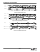
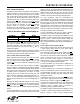
2.2. SSOP Typical Application Schematic
Notes:
1. Place C1 close to VA and C4 close to VD pin.
2. All grounds connect directly to GND plane on PCB.
3. Pins 6 and 7 are no connects, leave floating.
4. Pins 10 and 11 are unused. Tie these pins to GND.
5. To ensure proper operation and receiver performance, follow the guidelines in “AN383: Si47xx Antenna, Schematic,
Layout, and Design Guidelines.” Silicon Laboratories will evaluate schematics and layouts for qualified customers.
6. Pin 8 connects to the FM antenna interface, and pin 12 connects to the AM antenna interface.
7. Place Si473x-D60 as close as possible to antenna and keep the FMI and AMI traces as short as possible.
R3
R1
C3
L1
C9
T1
3
1
L2
C2
C4
C1
C3
R2
R2
C9
R1
C7
C8
R3
X1
2
1
C5
C6
13
14
15
16
17
18
19
20
21
22
23
24
12
11
10
9
8
7
6
5
4
3
2
1
DOUT
DFS
GPO3/DCLK
GPO2/INT
GPO1
NC
NC
FMI
RFGND
NC
NC
AMI
LOUT
ROUT
DBYP
VA
VD
RCLK
SDIO
SCLK
SENB
RSTB
GND
GND
Si473x
RFGND
AMI
GPO3 RCLK
RIN
DOUT
DOUT
DCLK
DFS
DFS
GP03/DCLK
LOUT
ROUT
LIN
OPMODE: 0xB0, 0xB5
Optional: AM Air Loop Antenna
Optional: For Crystal OSC
FM Antenna
Optional: AUXIN/Digital Audio Out
Si473x
2
1
VD
D60
3
24
23
OPMODE: 0x5B, 0x0B
Optional: Digital Audio Out
1.62 to 3.6 V
2.0 to 5.5 V
VA
DOUT
DFS
GPO3/DCLK
LOUT
ROUT
RCLK
SDIO
SCLK
SENB
RSTB
GPO1
GPO2/INT