
Specifications
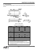


Si4730/31/34/35-D60
32 Rev. 1.1
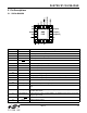
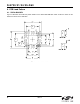
5.2. Si473x-D60-GU
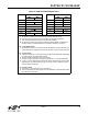
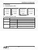
Pin Number(s) Name Description
1 DOUT/[LIN] Digital output data for digital output mode or Left channel input for AUX IN ADC
mode.
2 DFS/[RIN] Digital frame synchronization input for digital output mode or Right channel input
for AUXIN ADC mode.
3 GPO3/[DCLK] General purpose output, crystal oscillator, or digital bit synchronous clock input
in digital output mode.
4 GPO2/[INT]
General purpose output or interrupt pin.
5 GPO1 General purpose output.
6,7 NC No connect. Leave floating.
8 FMI FM RF inputs. FMI should be connected to the antenna trace.
9 RFGND RF ground. Connect to ground plane on PCB.
10,11 NC Unused. Tie these pins to GND.
12 AMI AM/SW/LW RF input.
13,14 GND Ground. Connect to ground plane on PCB.
15 RST
Device reset input (active low).
16 SEN
Serial enable input (active low).
17 SCLK Serial clock input.
18 SDIO Serial data input/output.
19 RCLK External reference oscillator input.
20
V
D
Digital and I/O supply voltage.
21
V
A
Analog supply voltage. May be connected directly to battery.
22 DBYP Bypass capacitor.
23 ROUT/[DOUT] Right audio line output in analog output mode.
24 LOUT/[DFS] Left audio line output in analog output mode.
LOUT/[DFS]
ROUT/[DOUT]
DBYP
VD
GPO2/[INT]
GPO3/[DCLK]
DOUT/[LIN]
DFS/[RIN]
1
2
3
4
5
6
7
8
9
10
11
12
GPO1
VA
SDIO
NC
NC
RCLK
SEN
FMI
RFGND
SCLK
GND
NC
NC
RST
GND
AMI
24
23
22
21
20
19
18
17
16
15
14
13