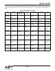
Si 4 7 x x - EVB Si47 XX E VALUATION B OA RD U SER ’ S G UIDE 1. Introduction Thank you for purchasing the Silicon Laboratories, Inc. Si47xx Evaluation Board (EVB). The EVB and associated software have been designed to speed up the overall development process. We look forward to working with you, and have posted support articles, answers to frequently asked questions, and application notes at www.mysilabs.com. Table 1 describes all of the available products and features in the Si47xx family.
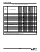
Si47xx-EVB Si4736 AM/FM/WB Receiver Si4737 AM/FM/WB Receiver with RDS Si4738 FM/WB Receiver Si4739 FM/WB Receiver with RDS Si47401 AM/FM Receiver AM/FM Receiver with RDS Si47421 AM/LW/SW/FM/WB Receiver Si47431 AM/LW/SW/FM/WB Receiver with RDS Si47441 AM/LW/SW/FM Receiver Si47451 AM/LW/SW/FM Receiver with RDS Si47491 High-Performance RDS Receiver Si4784 FM Receiver Si4785 FM Receiver with RDS
Si47xx-EVB TABLE O F C ONTENTS 1. Introduction . . . . . . . . . . . . . . . . . . . . . . . . . . . . . . . . . . . . . . . . . . . . . . . . . . . . . . . . . . . . .1 2. Description . . . . . . . . . . . . . . . . . . . . . . . . . . . . . . . . . . . . . . . . . . . . . . . . . . . . . . . . . . . . . .8 2.1. Si47xx Baseboard . . . . . . . . . . . . . . . . . . . . . . . . . . . . . . . . . . . . . . . . . . . . . . . . . . . .8 2.2. Si47xx Daughtercards . . . . . . . . . . . . . . . . . . . . . . . . .
Si47xx-EVB 7.3. Weather Band Settings Property Window . . . . . . . . . . . . . . . . . . . . . . . . . . . . . . . . . 92 7.4. Weather Band Receiver RSSI/SNR Graph Window . . . . . . . . . . . . . . . . . . . . . . . . . 94 7.5. Weather Band Receiver Register Map Window . . . . . . . . . . . . . . . . . . . . . . . . . . . . 95 7.6. Weather Band Receiver SAME Event Data (Si4707 only) . . . . . . . . . . . . . . . . . . . . 96 8. AM Receiver GUI . . . . . . . . . . . . . . . . . . . . . . . . . . . . . . .
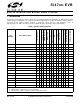
Si47xx-EVB This user's guide contains information related to only the Si47xx EVBs itemized in Table 2. Table 2 serves as a quick reference guide for the sections of interest for your EVB. Sections 1, 4, 9, and 10 of the document apply to all EVBs. Table 2. Quick Reference Guide Part Description Recommended HW Setup GUI Bill of Materials Schematics Layout Si4704/05/ 06/84/85 Sections 2.1., 2.2.1., and 2.2.6. Section 3.2. Section 6. Section 11. Tables Sections 12.1., Sections 29 and 30 12.2. 13.1.
Si47xx-EVB There are ten different EVB kits within the Si47xx family. Each kit ships with a standard set of components that are common to all kits and a unique set that depends on the EVB kit P/N. Standard set of components are: Customer welcome and evaluation letter Characterization Report USB cable RCA cable 9 V battery Headphones Si47xx CD including: EVB Data sheet Development application GUI rev 2.5.4 or later guide Quick start guide.
Si47xx-EVB Table 3. Si47xx-EVB Kit Unique Contents (Continued) Adapters EVB Kit Base Board Daughtercard Antenna Cards Antennas BNC Male to RCA Female SMA Male to BNC Female SMA Female to BNC Male SMA Male to SMA Male Si4735-EVB Si47xx Base board Rev1.3 or later Si473x Daughter Card Rev1.2 or later SW antenna Whip antenna Yes No No No Si4737-EVB Si47xx Base board Rev1.3 or later Si473x Daughter Card Rev1.
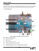
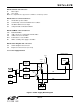
Si47xx-EVB 2. Description Si47xx EVB consists of a baseboard, a daughtercard with the Si47xx part pre-mounted, and, if applicable, an antenna card. The baseboard is common and shared among all Si47xx EVBs. The following sections refer to both the images in the figures and the silkscreen on the Si47xx EVB. Please refer to both when using this guide. 2.1. Si47xx Baseboard J6 J27 J30 J52 J57 X1 J61 J54 J68 J69 J75 J76 U22 D1 J79 J74 PB1 SW1 J78 Figure 1.
Si47xx-EVB Baseboard audio I/O connectors: J6 J30 RCA output Line output Note: Line output will not be supported on new EVBs as of February 14, 2011. Baseboard clock connectors/devices: X1 32.
Si47xx-EVB The Si47xx EVB can be powered using one of the following power supply options: 1. USB power supply via J79 2. External dc (Ext DC) power supply via power jack J78 or battery via J77 3. Three separate power supplies (Vdd, Vio, Vmcu) via terminal block J76 The EVB has three supply rails: Vdd, Vio, and Vmcu. Vdd and Vio are routed directly to the daughtercard to power the Vdd and Vio pins on the Si47xx chip, while Vmcu is used to power the baseboard.
Si47xx-EVB 2.1.2. Microcontroller TC_BCLK (reserved for digital Rx ) Jumper J41 Daughterboard S_GPO3/DCLK MD_GPIO3 MS_GPIO2 MD_GPIO1 J79 USB J74 JTAG GPO1 GPO2 GPO3/ DCLK Jumper J65 MCU C8051F342 PB1 Reset SD_GPO1 MD_GP4 19 18 17 MS_RSTB RST~ 5 Si47xx SEN~ SCLK SDIO 6 7 8 MS_SENB MS_SCLK MS_SDIO Figure 5. MCU Block Diagram The Si47xx EVB uses a Silicon Laboratories' C8051F342 microcontroller to control the Si47xx and to provide USB connectivity from the host PC (via connector J79).
Si47xx-EVB 2.1.3. Reference Clock Daughterboard Jumper J57 X1 32.768 kHz INT RClk DIS_INT_RCLK Si47xx INT_RCLK 9 RCLK Jumper J52 EXT_RCLK J54 EXT RClk Figure 6. Reference Clock Block Diagram The Si47xx accepts a 32.768 kHz reference clock at the RCLK pin. On the EVB, this clock is provided by a precision crystal oscillator. The user has the option of not using the onboard oscillator and bringing in the reference clock from an external source through SMA connector J54.
Si47xx-EVB The EVB supports three different kinds of configurations for the FM transmitter: Analog In to Analog In In to Digital In Digital In to Digital In Analog Analog In to Analog In: This configuration provides a way for the user to evaluate the analog audio input for FM transmission. The input to the EVB is an analog audio provided via the RCA input connector J7 or LINE In connector J19 (white). Jumpers J5 and J13 are set to RCA input by default.
Si47xx-EVB IMPORTANT: Jumper Settings Because of the many possibilities available to configure the EVB, ensure that these four jumpers are set accordingly: 1. J41: GPO3/DCLK setting 2. J44: TX/RX setting for Audio1 I/O (automatically set by the GUI for baseboard 1.3 and later) 3. J45: TX/RX setting for Audio2 I/O (automatically set by the GUI for baseboard 1.3 and later) 4.
Si47xx-EVB 2.2. Si47xx Daughtercards 2.2.1. Si471x/2x Daughtercard Figure 8.
Si47xx-EVB Figure 9. Fully Assembled Si471x/2x EVB Si470x/1x/2x EVBs use Si471x/2x daughtercard with different population options depending on the individual Si470x/1x/2x part. Please refer to individual Bill of Materials for each board. 16 Rev. 0.
Si47xx-EVB 2.2.2. Si473x Daughtercard Figure 10.
Si47xx-EVB Figure 11. Fully Assembled Si473x-EVB with Ferrite Antenna Card The Si473x/07 EVBs use Si473x daughtercard with different population options depending on the individual Si473x/07 part. Please refer to individual Bill of Materials for each card. Table 4 shows the antenna and audio connections for the Si47xx EVBs. 18 Rev. 0.
Si47xx-EVB 2.2.3. Si474x Daughtercard Figure 12. Si474x Daughtercard Connectors and Devices Daughtercard connectors and components: J4 BNC connector for antenna connection C6, C1, C18 Vdd bypass capacitor C2 FM matching component L1, L5 FM matching component Q1–2 Cascode amplifier for AM front-end boost circuit. U1 Si4740/41/42/43 AM/FM Receiver chip The daughtercard implements the Si4740/41/42/43 AM/FM RDS receive solution.
Si47xx-EVB Figure 13. Fully Assembled Si474x-EVB 20 Rev. 0.
Si47xx-EVB 2.2.4. Si4749 Daughtercard Figure 14. Si4749 Daughtercard Connectors and Devices Daughtercard connectors and components: J1 SMA connector for pass-thru FM connection J2 SMA connector for FM antenna connection C2 Vdd bypass capacitor L1 FM matching component U2 Si4749 RDS Receiver The daughtercard implements the Si4749 RDS receive solution. The SMA connector, J2, allows the user to attach a whip antenna for FM reception or a signal generator for FM test circuit.
Si47xx-EVB Figure 15. Fully Assembled Si4749-EVB 22 Rev. 0.
Si47xx-EVB 2.2.5. Antenna Interfaces 2.2.5.1. AM Antenna Interface Figure 16. Antenna Board Options—SL4X30MW100T (Medium Ferrite), SL5X7X100MW70T (Large Ferrite), and SL9X5X4MWTF Airloop The user has the flexibility of choosing one of the two available antenna options. The user can either decide to use the airloop antenna or the ferrite loop stick antenna. Rev. 0.
Si47xx-EVB 2.2.5.2. SW and Weather Band Antenna Interfaces Figure 17. SW/WB Antenna Card (SW Population) and (WB Population) The BNC connector, J2, will be used to connect a whip antenna for shortwave, FM, and weather band reception. For SW reception, switch S1 must be in the SW position. The ferrite bar is used for AM reception, and the switch S1 must be in the AM position for AM reception. When using the WB Antenna Card, WB reception is through the whip antenna.
Si47xx-EVB Table 4.
Si47xx-EVB Table 4. Si47xx Antenna Connections (Continued) EVB Kit Name Receiver AM Antenna Options FM Antenna Options FM Connections Whip/WB Antenna Card J2 AM Connections SW Antenna Options SW Connections Si4743-CEVB Si4743 Whip / Si474x Antenna Dummy card J4 Whip J4 Whip Si4749-CEVB Si4749 None None Whip J2 None WB Antenna Options WB Connections Whip/WB Antenna Card. For WB reception, set the S1 switch to WB position J2 Table 5.
Si47xx-EVB 2.2.6. Test Circuit Interfaces Table 6 shows the test circuit interface connections for Si47xx EVBs. Table 6. Si47xx Test Circuit Connections EVB Kit Name Receiver AM/SW/LW Test Options AM/SW/LW Connections FM Test Options FM Connections Audio Out Test Options Audio Out Connections Audio In Test Options Audio In Connections Si4705-X-EVB Si4705 None None FMI / SMA J28 through C1.
Si47xx-EVB 3. Recommended Hardware Setup The Si47xx-EVB can be configured for FM transmit, FM receive, WB receive, or AM/SW/LW receive. The following is a description of how to correctly configure the device for either mode of operation. 3.1.
Si47xx-EVB 3.2. Hardware Setup for FM or Weather Band Receiver Test RF Generator SMA Cable Audio Analyzer RCA Cable J6 J28 or J26 FM IN J7 RCA OUT Optical Cable RCA IN J19 Si47xx Daughterboard Jumpers Setting DCLK TX GPIO3 J41 RX RX J44 J45 S/PDIF OUT TX J30 Note: J44 and J45 are automatically configured in EVB Rev1.3 and later J76 Si47xx Baseboard Terminal Block (TB) SW1 USB EXT pwr J79 USB pwr J78 EXT Jack USB Cable PC w/ USB port Figure 20.
Si47xx-EVB 3.3. Hardware Setup for AM Receiver Test Audio Analyzer RCA Cable J6 J28 or J26 J24 FM IN J7 RCA OUT Optical Cable RCA IN J19 Si473x J1 Daughterboard RF Generator Jumpers Setting SMA Cable DCLK TX GPIO3 J41 RX RX J44 J45 S/PDIF OUT TX J30 Note: J44 and J45 are automatically configured in EVB Rev1.3 and later J76 Si47xx Baseboard Terminal Block (TB) USB SW1 EXT pwr J79 USB pwr J78 EXT Jack USB Cable PC w/ USB port Figure 21.
Si47xx-EVB Audio Analyzer/ Amplifier RCA Cable J6 RCA OUT Optical Cable RF Generator Antenna Dummy AM IN J4 J19 Si474x Daughterboard S/PDIF OUT AM Test Setup J30 Si47xx Baseboard J76 Terminal Block (TB) SW1 USB EXT pwr J79 USB pwr J77 EXT Jack USB Cable PC w/ USB port Figure 22. Hardware Setup for AM Receiver Test (Si474x) Instructions for Si474x daughtercards: 1. Connect the USB cable from PC to the EVB USB connector, J79.
Si47xx-EVB 4. Getting Started 4.1. Software Installation The Si47xx Windows GUI (graphical user interface) software is designed for use with the Si47xx evaluation board (EVB). The GUI software revision number is available under HelpAbout. The GUI software development program uses a host machine USB port to communicate with the Si47xx EVB and is tested for use with Windows XP, Windows 2000, and Windows 7.
Si47xx-EVB 4.2. Board Initialization After launching the GUI, you will be shown the initialization window as shown in Figure 25. Note: This window can be accessed at any time by choosing Initialize from the File menu from the main GUI screen. Figure 25. GUI Initialization Screen 4.2.1. Board Selection At the top of the initialization window there is a board selection box, as displayed in Figure 26, that allows the selection of the board that will be controlled by the GUI.
Si47xx-EVB 4.2.2. Board Discovery Bus Mode The initialize process can be configured to use either 2-wire or 3-wire bus mode. This can be configured by selecting File Board Discovery Bus Mode. This feature is useful when using the Silabs EVB and GUI to control a prototype that is designed to use one bus mode only. 4.2.3. Function Configuration For each mode available on the selected EVB, multiple configuration items (Figure 27) will be present to allow for configuration of the GUI software.
Si47xx-EVB 4.2.3.3. Default Mode There are two or more default modes possible for each function. Use Last UI State: When selected, the GUI will restore all settings on the device to the previous settings configured in the GUI the last time it was closed. Use Chip Defaults: When selected, the GUI will use the settings that were default in the firmware on the device.
Si47xx-EVB 4.2.3.6. Bus Mode This setting affects all functions that are configured. It allows the device to be booted either in 2-wire or 3-wire mode. 4.2.3.7. Internal Oscillator When the "Use XOSCEN" is enabled and the board is configured to use the crystal oscillator, the GUI will boot the device using the crystal oscillator. This option is only available on devices that support the crystal oscillator option. 4.2.3.8.
Si47xx-EVB 4.4. State Management Once the part has been initialized, a State Management option becomes available in the File Menu. This GUI feature allows the user to save, retrieve, load, and delete the configuration state which contains the property values. 4.4.1. Save Configuration State To save the current configuration state, select FileState ManagementSave Current State. The Select Configuration window shown in Figure 30 will pop up. Enter a name for the configuration state and click OK.
Si47xx-EVB 4.4.3. Load Configuration State When a configuration state for a part has been saved, it will also appear in the Load State list as shown in Figure 32. Select the state you wish to load, and all properties and the tuning frequency of the saved configuration will be restored without doing initialization to the chip. Figure 32. Loading Configuration State 4.4.4. Delete Configuration State To discard a saved configuration state, select FileState ManagementDelete State.
Si47xx-EVB 4.4.5. Export Saved State In addition to saving, retrieving, and deleting the configuration state, the GUI also gives the end user the ability to export the configuration state to a file. The file can then be imported to installations of the GUI on different machines to allow multiple users to easily implement the same configuration state.
Si47xx-EVB 5. FM Transmitter GUI The first Si47xx window is the Initialization window as shown in Figure 35. Select the FM transmitter function. As an FM transmitter, there are three audio input settings available: Analog Input Analog to Digital Input Digital Input 5.1. Configuring the Si47xx as an FM Transmitter Using Analog Audio Input This mode configures the Si47xx to receive analog audio input at pins 15 and 16 (LIN and RIN).
Si47xx-EVB 5.2. Configuring the Si47xx as an FM Transmitter Using Digital Audio with Analog Audio Source This mode configures the Si47xx to receive digital audio input at pins 13 and 14 (DIN and DFS), but the user still provides an analog audio source to the EVB. It is useful for a user who wants to test digital input on the Si47xx but does not have a digital audio source.
Si47xx-EVB 5.3. Configuring the Si47xx as an FM Transmitter Using Digital Audio with SPDIF Digital Source This mode configures the Si47xx to receive digital audio input at pin 13 and 14 (DIN and DFS) when the user has an SPDIF digital audio source. The SPDIF source is converted to PCM digital audio by the SPDIF translator. Refer to Figure 42, “SPDIF Settings Property Window,” on page 50 to control the SPDIF translator.
Si47xx-EVB 5.4. FM Transmitter Main Window The FM transmitter main window will appear after initialization. 26 1 5 4 2 3 8 7 18 13 9 10 19 14 11 12 17 20 21 15 16 22 24 25 23 6 Figure 38. FM Transmitter Main Window Table 8. FM Transmitter Main Window Descriptions # Description Range 1 Transmit frequency display. Enter the desired FM transmit frequency in this window. 76–108 MHz 2 Transmit voltage display. Enter the desired FM transmit voltage in this window.
Si47xx-EVB Table 8. FM Transmitter Main Window Descriptions (Continued) # Description 11 RDS Deviation. Enter the desired RDS deviation in this window (Si4711/13/21 only). Range 0–7.5 kHz 12 Total Deviation. This is an indicator only displaying the sum of the audio, pilot and RDS deviation. If the total deviation exceeds 75 kHz, the indicator will turn red and a warning sign is displayed. 0–187.5 kHz 13 Input Mute Left/Right. Selecting this checkbox will mute the Left or Right audio channel.
Si47xx-EVB 5.5. FM Transmitter Settings (Analog Mode) Property Window FM transmitter settings can be configured through the properties window by selecting WindowProperties. Properties are grouped into categories which can be selected from the drop-down box in the upper right of the window. For convenience, all FM transmitter properties are also located in WindowPropertiesTX: All. Analog mode properties will be available if Analog Mode was selected in the initialization window. Figure 39.
Si47xx-EVB Table 9. FM Transmitter Settings in Analog Mode Property Window Descriptions (Continued) Item Description Range Devices Reference Clock Prescaler This field is used to specify the prescaler value. The input to the RCLK pin divided by the prescaler is the reference clock. The reference clock must be in the range of 31130 to 34406 Hz. 1–4095 All Audio Level High Duration (mSec) Set the duration for the audio level high before an interrupt is generated.
Si47xx-EVB 5.6. FM Transmitter Settings (Digital Mode) Property Window FM transmitter settings can be configured through the properties window by selecting WindowProperties. Properties are grouped into categories which can be selected from the drop-down box in the upper right of the window. For convenience, all FM transmitter properties are also located in WindowProperties TX: All. Digital mode properties will be available if CODED or SPDIF modes was selected in the initialization window. Figure 40.
Si47xx-EVB Table 10. FM Transmitter Settings in Digital Mode Property Window Descriptions (Continued) Item Description Range Applicable Devices Digital Mono Mode Enable Select between Digital Stereo or Mono. On/Off All Digital DCLK Falling Edge Select between using rising edge or falling edge of DCLK when sampling Digital Input (DIN) data.
Si47xx-EVB 5.7. CODEC Settings In addition to other digital mode properties, a category of CODEC settings may configured by selecting WindowPropertiesCODEC Settings if CODEC mode was selected in the initialization window. Figure 41. CODEC Settings Property Window Table 11. CODEC Settings Property Window Descriptions Item Description Range Misc. CODEC Precision 16, 20, 24 bits Select the CODEC digital audio output precision.
Si47xx-EVB 5.8. SPDIF Settings In addition to other digital mode properties, a category of SPDIF settings may be configured by selecting WindowPropertiesSPDIF Settings if SPDIF mode was selected in the initialization window. Note: SPDIF will not be supported on new EVBs as of February 14, 2011. These properties will not be available through the GUI in conjunction with those boards. Figure 42. SPDIF Settings Property Window Table 12.
Si47xx-EVB 5.9. FM Transmitter Receive Power Scan Window The Receive Power Scan window enables the user to scan the entire FM band to find one or more candidate channels on which to transmit, where candidate channels are defined as those with the lowest received power. Selecting WindowPower Scan will launch the Receive Power Scan Window as shown in Figure 43. The band and channel spacing can be selected and the number of regions can be set to return one to ten candidate channels.
Si47xx-EVB 5.10. FM Transmitter Radio Data Service (RDS) The RDS/RBDS feature is available with the Si4711/13/21. This user guide assumes that the user is already familiar with the RDS/RBDS standard. If necessary, the user may refer to the following documents to become familiar with the RDS/RBDS standard. United States RBDS Standard by National Radio Systems Committee, April 9, 1998. RDS Universal Encoded Communication Protocol Version 5.1 by European Broadcasting Union, August 1997.
Si47xx-EVB Figure 45. RDS Transmit Window Table 13. RDS Transmit Window Descriptions Item Description General RDS/RBDS Selection Select either RDS format (Europe) or RBDS format (US). Program Type (PTY) Select the available Program Type (PTY) from the pulldown menu. PTY Dynamic PI Select whether the PTY will be dynamic or static. Enter Program Identification (PI) code here. Program Service Program Service Messages Enter up to 12 different Program Service (PS) Messages.
Si47xx-EVB Table 13. RDS Transmit Window Descriptions Item Stereo Audio Compression Description Part of RDS Group Type 0 (PS): Enter whether the transmitted audio is Stereo or Mono. Part of RDS Group Type 0 (PS): Enter whether the Audio Compression is On or Off. Traffic Program Part of RDS Group Type 0 (PS): Enter whether Traffic Program is available or not. Traffic Announcement Part of RDS Group Type 0 (PS): Enter whether Traffic Announcement is available or not.
Si47xx-EVB There are 16 different group types in the RDS/RBDS standard, and for every group the following information is always transmitted: 1. Program Identification (PI) 2. Program Type (PTY) The GUI makes it easy to send data in three of the following group types: 1. Group Type 0: Program Service (PS) 2. Group Type 2: Radio Text (RT) 3. Group Type 4: Clock Time (CT) It is possible to send data in the other group types, but the user has to manually enter the data in hexadecimal code.
Si47xx-EVB 5.10.1. Basic The RDS Transmit Window is divided into three categories: 1. General 2. Program Service 3. Buffers In the basic section, we will cover two out of the three categories: the General and Program Service. In the General category, the user can set the PI and PTY data. In the Program Service, the user can set the PS data (Group Type 0). The following diagram shows a step-by-step explanation: 1 2 3 4 5 Figure 46. Basic RDS Message Illustration 1.
Si47xx-EVB 5.10.2. Intermediate In the intermediate section, we will cover the buffers category of sending the RDS data with the device, in particular we will send Group Type 2 (Radio Text) and Group Type 4 (Clock Time). The following diagram shows a step-by-step procedure to send the buffers data in addition to the General and Program Service data covered in the basic section. 1 2 3a 3 5 6 4 Figure 47. Intermediate RDS Message Illustration 1.
Si47xx-EVB value is set to anything other than 100%. 5. Clicking the "Add Time" button here will add the current time as a RDS Group Type 4 message to the GUI FIFO Buffer queue. 6. Clicking the "Clear Buff & Send" button will upload the message from the FIFO Buffer Indicator Window into the FIFO Buffer inside the device. The FIFO Buffer on the part will only send the messages contained in the buffer once. A good example of using FIFO buffer is when you want to send the time data.
Si47xx-EVB uploaded means that the RT is uploaded with the flag set. Un-checking this box when an RT is uploaded means that the flag is not set. This flag tells the receiver that when the flag toggles from set to reset or vice versa, the receiver will clear the display before showing the next RT. 5. Manual Group Entry: Use this box to upload the RDS data manually. You can use this box to upload messages from the Group Type for which the GUI does not have encoding support.
Si47xx-EVB 5.11. FM Transmitter Register Map Window The register map window allows the user to manually program the device by sending commands to the chip. Refer to “AN332: Si47xx Programming Guide” to manually program the device. Clicking on WindowRegister Map will launch the Register Map Window as shown in Figure 49. Figure 49. FM Transmitter Register Map Window 60 Rev. 0.
Si47xx-EVB 6. FM Receiver GUI The first Si47xx window is the Initialization window as shown in Figure 50. Select the FM receiver function. As an FM receiver, analog audio out is available on pins 13 and 14. 6.1. Configuring the Si47xx as an FM Receiver Select the device, busmode, firmware revision, and initial part settings and then click Initialize. A new window displaying "Initializing FM Receiver" will appear.
Si47xx-EVB 6.2. FM Receiver Main Window The FM receiver main window will appear after initialization. 11 3 2 5 4 6 Figure 51. FM Receiver Main Window Figure 52. FM Receiver Main Window for Si474x 62 Rev. 0.
Si47xx-EVB Table 14. FM Receiver Main Window Descriptions # Name Descriptions 1 Tune/Seek Tune Down (<), Tune Up (>) buttons execute a single channel step according to the channel spacing setting. The channel spacing setting can be set in the property window. Seek down (<<), Seek Up (>>) buttons execute a seek up or down to the next received FM signal meeting or exceeding the seek settings within the selected band.
Si47xx-EVB 6.3. FM Receiver Settings Property Window FM receiver settings can be configured through the properties window by selecting WindowProperties. Properties are grouped into categories which can be selected from the drop-down box in the upper right of the window. For convenience, all FM receiver properties are also located in WindowPropertiesFM: All. Figure 53. FM Receiver Settings Property Window 64 Rev. 0.
Si47xx-EVB Figure 54. FM Receiver Setting Property Window for Si474x (1 of 2) Rev. 0.
Si47xx-EVB Figure 55. FM Receiver Setting Property Window for Si474x continued (2 of 2) 66 Rev. 0.
Si47xx-EVB Table 15. FM Receiver Settings Property Window Descriptions Items Range Applicable Devices Larger values provide slower attack and smaller values provide faster attack. 4–248 Si474x AGC Index If AGC override is set to “ON,” this property will determine the AGC setting. 0–26 All AGC Override If set to “ON,” the AGC property will be used to set the value of the AGC. If set to “OFF,” the AGC setting will be automatically determined by the part.
Si47xx-EVB Table 15. FM Receiver Settings Property Window Descriptions (Continued) Items Range Applicable Devices 8-bit, 16-bit, 20bit, 24-bit Si4705/06, Si4721/31/35/37/39, Si4730/34/36/38-D60 and later, Si4741/43/45, Si4784/85 Digital Sample Rate DFS sample rate for digital input signal. Hz Recommended values are: 32 kHz, 44.1 kHz, or 48 kHz. Over-sampling rate must be set in order to satisfy a minimum DCLK of 1 MHz. Sample rate must be set to 0 before DCLK/DFS is removed.
Si47xx-EVB Table 15. FM Receiver Settings Property Window Descriptions (Continued) Items Description Range Applicable Devices Hi-Cut SNR High Threshold Sets the SNR level at which hi-cut begins to band limit. 0 – 127 dB Si4740/41/42/43/44/45, Si4704/05-D50 and later, Si4706-C30 and later, Si4730/31/34/35/84/85-D50 and later Hi-Cut SNR Low Threshold Sets the SNR level at which hi-cut reaches maximum band limit.
Si47xx-EVB Table 15. FM Receiver Settings Property Window Descriptions (Continued) Items Description Range Applicable Devices Seek Band Top (MHz) The upper frequency limit for the seek function. This is set automatically by the GUI based on band and spacing selection. US: 107.9 MHz (200 kHz spacing) Europe: 108 MHz (100 kHz spacing) Japan: 90 MHz Japan Wide: 108 MHz All Max Tune Error (kHz) Selects the maximum tuning frequency error before the AFC rail indicator is set.
Si47xx-EVB Table 15. FM Receiver Settings Property Window Descriptions (Continued) Items Description Range Applicable Devices Blend Multipath Attack Rate Attack rate associated with multipath when adjusting blend. If set to 0, attack would be disabled. 0–32767 Si4740/41/42/43/44/45, Si4704/05-D50 and later, Si4706-C30 and later, Si4730/31/34/35/84/85-D50 and later Blend Multipath Mono Threshold Multipath input level above which the tuner blends into full mono.
Si47xx-EVB Table 15. FM Receiver Settings Property Window Descriptions (Continued) Items Description Range Applicable Devices 0–32767 Si4740/41/42/43/44/45, Si4704/05-D50 and later, Si4706-C30 and later , Si4730/31/34/35/84/85-D50 and later 0–127 dB Si4740/41/42/43/44/45, Si4704/05-D50 and later, Si4706-C30 and later , Si4730/31/34/35/84/85-D50 and later Stereo Blend Mono RSSI threshold below which the tuner Threshold (dB) blends into full mono.
Si47xx-EVB 6.4. CODEC and SPDIF Settings Si47xx-EVB baseboard has a Codec and an SPDIF translator for digital audio output. For tuners with digital audio option, you can set properties for the Codec and SPDIF through the GUI. These settings can be used with AM or FM tuners that have digital audio enabled. Select WindowPropertiesCODEC and SPDIF Settings. Note: SPDIF will not be supported on new EVBs as of February 14, 2011.
Si47xx-EVB 6.5. FM Receiver RDS Window The FM receive RDS window allows the user to view program service, program type, PI code, radio text, enhanced radio text, radio text plus, clock, group error rate, sync time and display times, an alternate frequency list, and group statistics. Select WindowRDS Receive Data. Click on Radio Text Plus (RT+) to get the RT+ class and item information. 2 1 6 4 3 7 5 8 Figure 57. FM Receiver Settings RDS Window 74 Rev. 0.
Si47xx-EVB Table 17. FM Receiver Settings RDS Window Descriptions # 1 Items Description Radio Data Service PS: Program Service Indicator (8 characters). RT: Radio Text Indicator (64 characters). eRT: Enhanced Radio Text Indicator CT: Clock Indicator showing time, day, and date. Group Error Rate indicates the percentage of uncorrectable groups received. PTY: Program Type Indicator PI: PI Code Indicator 2 Sync Times 3 Indicates that RDS is synchronized.
Si47xx-EVB Figure 58. RDS Group Counters Window 76 Rev. 0.
Si47xx-EVB 6.6. FM Receiver RDS Settings RDS settings are configured by selecting WindowPropertiesFM Receiver RDS Settings. Figure 59. FM Receiver RDS Settings Window Rev. 0.
Si47xx-EVB Table 18. FM Receiver RDS Settings Window Descriptions Item Description Range Misc. RDS State Enables and disables RDS. On, Off RDS Error Checking (RT and PS) Selects GUI error checking level. Minimum displays text as received. Mid-range requires two duplicate buffers before displaying text. Maximum requires two duplicate buffers and also ignores the A/B flag. Minimum, Mid-Range, Maximum RDS Program Type Decode Selects RDS or RBDS program type RDS, RBDS decoding.
Si47xx-EVB 6.7. FM UI Settings Figure 60. FM UI Settings Property Window Table 19. FM UI Settings Property Window Descriptions Hems Description Range Misc. 0.2–4.0 seconds Update Rate (sec) The time span when the UI gets status information from the part. Scan Time 1 (sec) In log band scan, the time between seeking and retrieving data from the UI. 1–10 seconds Scan Time 2 (sec) In log band scan, the time it takes the RDS data to populate, if RDS is available.
Si47xx-EVB 6.8. FM Receiver RSSI/SNR Graph Window The RSSI/SNR Graph Window allows the user to plot RSSI and SNR across the FM band. Bitmap data can be saved to file by selecting FileSave as Bitmap and tabulated data can be saved to file by selecting FileSave to .csv. 1 3 2 4 5 6 Figure 61. FM Receiver RSSI/SNR Graph Window Table 20.
Si47xx-EVB 6.9. FM Receiver Register Map Window The register map window allows the user to manually program the device by sending commands to the device. Refer to "AN332: Si47xx Programming Guide" to manually program the device. Figure 62. FM Receiver Register Map Window Rev. 0.
Si47xx-EVB 6.10. FM Receiver Logging Tools The GUI provides several useful logging tools. In the tools menu, user can choose to log raw RDS data, band scan data, device commands and channel info. Figure 63. Logging Tools 6.10.1. Log Band Scan Selecting ToolsLog Band Scan allows you to specify a filename and begin a scan of the entire band for RDS data, RDS acquisition times, and the contents of each register.
Si47xx-EVB 6.11. FM Receiver Configuration Helper The configuration helper is a useful tool for configuring the thresholds related to RSSI based Blend, SNR based Blend, Multipath based blend, SNR based hi-cut, Multipath based hi-cut, and Soft Mute. Figure 64. FM Configuration Helper 1 2 3 4 5 6 Figure 65. FM Configuration Helper Window (Multipath Based Hi-cut) Rev. 0.
Si47xx-EVB Table 21. Configuration Helper Window Descriptions # Item Description 1 Select Parameter Selects between Hi-cut Multipath (Si4706/4x only), Hi-cut SNR(Si4706/ 4x only), SoftMute, Stereo blend Multipath (Si4706/4x only), Stereo Blend RSSI and Stereo Blend SNR (Si4706/4x only). 2 Hi-cut/ Blend/Soft Mute Graph The plot displays the device threshold and rate settings, current signal conditions, and the calculated audio conditioning.
Si47xx-EVB Figure 66. FM Configuration Helper Window (SNR Based Hi-cut) In the example shown in Figure 66, the current level marker shows that hi-cut filter is set at 6 kHz. This is determined by both SNR and multipath conditions. Current SNR is 5 dB. Hi-cut SNR Low Threshold is set at 15 dB and hi-cut minimum frequency is set at 6 kHz. SNR is the determining factor in this case as it is already lower than the low threshold.
Si47xx-EVB Figure 67. FM Configuration Helper Window (Softmute) In the example shown in Figure 67, the current level marker shows that Soft Mute level is 0 dB. SNR threshold is programmed as 4 dB and max attenuation is 16 dB. Since the SNR reported by the part is 5 dB, which is above the threshold, the softmute level is 0 dB. The graph shows the current state of SNR (green diamond) and plot shows the softmute profile based on max attenuation, threshold and slope settings.
Si47xx-EVB Figure 68. FM Configuration Helper Window (SNR Based Blend) In the example shown in Figure 68, the Current Level marker shows that Stereo % is 56%. SNR threshold is programmed as 14 dB (and below) for full mono and 30 dB (and above) for full stereo. Since the SNR reported by the part is in between the thresholds, the stereo level is 56%. RSSI and Multipath do not factor in here as they are both at levels that would set the part in full stereo.
Si47xx-EVB Figure 69. FM Configuration Helper Window (RSSI Based Blend) In the example shown in Figure 69, the Current Level marker shows that Stereo % is 56%. RSSI threshold is programmed as 30 dBµV (and below) for full mono and 49 dBµV (and above) for full stereo. RSSI reported by the part is in between the thresholds however the final blend percentage is determined by SNR and the stereo level is 56%. Multipath does not factor in here as it is at a level that would set the part in full stereo.
Si47xx-EVB In the example shown in Figure 70, the Current Level marker shows that Stereo % is 50%. Multipath threshold is programmed as: 60% (and above) for full mono and 20% (and below) for full stereo. Multipath reported by the part is 11% which would put the part in full stereo. However the final blend percentage is determined by SNR and the stereo level is 56%.
Si47xx-EVB 7. Weather Band GUI 7.1. WB Receiver Initialization The first Si47xx window is the Initialization window as shown in Figure 71. On the function menu, select and highlight the function of the Si47xx as a WB Receiver. Select the Boot Mode, Audio Mode, Firmware, Bus Mode, and initial part settings and then click Initialize. A new window displaying "Initializing WB Receiver" will appear. If you check "Use XOSCEN," the daughter card crystal and on-chip oscillator will be used to clock the Si47xx.
Si47xx-EVB 7.2. Weather Band Main Window The weather band main window will appear after initialization. 2 1 3 5 7 4 6 8 Figure 72. Weather Band Receiver Main Window Table 22. Weather Band Receiver Main Window Descriptions # Name Description 1 Tune/Seek Tune Down (<), Tune Up (>) buttons execute a signal channel step (25 kHz step). Seek function is not available in the WB Receiver mode. 2 Frequency Slider Bar, AFC Valid, Alert Tone The Frequency Display indicates the frequency in MHz.
Si47xx-EVB 7.3. Weather Band Settings Property Window WB receiver settings can be configured through the properties window by selecting WindowProperties. Properties are grouped into categories which can be selected from the drop-down box in the upper right of the window. For convenience, all WB receiver properties are also located in WindowPropertiesWB: All. Figure 73. Weather Band Receiver Settings Property Window Table 23.
Si47xx-EVB Table 23. Weather Band Receiver Settings Property Window (Continued) Item Description Digital Sample Rate Hz DFS sample rate for digital input signal. Recommended values are: 32 kHz, 44.1 kHz, or 48 kHz. Over-sampling rate must be set in order to satisfy a minimum DCLK of 1MHz. Sample rate must be set to 0 before DCLK/DFS is removed. Digital Mono Mode Enable ON enables mono in digital audio output. Digital DCLK Falling Edge ON uses falling edge of DCLK for sampling.
Si47xx-EVB 7.4. Weather Band Receiver RSSI/SNR Graph Window The RSSI/SNR Graph Window allows the user to plot RSSI and SNR across the weather band. Bitmap data can be saved to file by selecting FileSave as Bitmap and tabulated data can be saved to file by selecting FileSave to .csv. 1 2 3 4 Figure 74. Weather Band Receiver RSSI/SNR Graph Window Table 24.
Si47xx-EVB 7.5. Weather Band Receiver Register Map Window The register map window allows the user to manually program the device by sending commands to the device. Refer to "AN332: Si47xx Programming Guide" to manually program the device. Figure 75. Weather Band Receiver Register Map Window Rev. 0.
Si47xx-EVB 7.6. Weather Band Receiver SAME Event Data (Si4707 only) The SAME Event Data window allows the user to view the SAME message description, originator ID, originator type, purge time, origination time, region along with the raw data and event confidence. The Event to be displayed can be selected through the "Event" drop down box. The message buffer can be cleared by clicking on the "Clear Messages" button.
Si47xx-EVB 8. AM Receiver GUI 8.1. AM Receiver Initialization The first Si474x window is the Initialization window as shown in Figure 77. On the function drop-down menu, select the function of the Si474x as an AM Receiver. Select the device, busmode, firmware revision, and initial part settings and then click Initialize. A new window displaying "Initializing AM Receiver" will appear. Crystal operation is not supported on Si474x-EVB (that supports Si4740/41/42/43/44/45).
Si47xx-EVB 8.2. AM Receiver Main Window The AM receiver main window will appear after initialization. Figure 78. AM Receiver Window Table 25. AM Receiver Window Descriptions # Name Description 1 Tune/Seek Tune Down (<), Tune Up (>) buttons execute a single channel step according to the channel spacing setting. The channel spacing setting can be set in the property window.
Si47xx-EVB Table 25. AM Receiver Window Descriptions (Continued) # Name Description 6 Status The RSSI indicator displays the RSSI of the signal in dBuV. The SNR indicator displays the SNR of the received signal in dB. The varactor value specifies the capacitance of the tuning front-end. A value of 6143 means that the maximum capacitance is being presented at the AM input and a value of 1 means that the varactor is at its minimum value. The AGC Index indicator displays the AGC status.
Si47xx-EVB 8.3. AM Receiver Property Settings Window AM receiver settings can be configured through the properties window by selecting WindowProperties. Properties are grouped into categories which can be selected from the drop-down box in the upper right of the window. For convenience, all AM receiver properties are also located in WindowPropertiesAM: All. Figure 79. AM Receiver Settings Property Window 100 Rev. 0.
Si47xx-EVB Figure 80. AM Receiver Settings Property Window for Si474x Rev. 0.
Si47xx-EVB Table 26. AM Receiver Property Window Descriptions Name Description AGC Attack Rate Sets the AGC attack rate. Larger values provide slower attack and smaller values provide faster attack. AGC Frontend Sets gain index backup (ATTN_BACKUP) for exterAttn. Backup nal attenuator. For Si4743EVB, 12 and 20 are recomSteps mended for "Passive" and "Active" external attenuators, respectively. AGC Frontend Sets minimum gain index. For Si4743EVB, 19 is recMin. Gain Index ommended.
Si47xx-EVB Table 26. AM Receiver Property Window Descriptions (Continued) Name Digital Format Description Range Applicable Devices I2S, Left-Justified, DSP Si4705/06, Si4731/35/37/39, Si4730/34/36/38D60 and later, Si4741/43/45, Si4784/85 Digital Mono ON, OFF Si4705/06, ON enables mono in digital audio output. Mode Enable Si4731/35/37/39, Si4730/34/36/38D60 and later, Si4741/43/45, Si4784/85 Digital Sample Digital audio output bit precision.
Si47xx-EVB Table 26. AM Receiver Property Window Descriptions (Continued) Name Description Seek Mode Seek mode specifies the behavior of seek when it reaches either end of the AM band. The default value makes the seek wrap around and start at the other end of the AM band. The other option makes seek stop if it reaches either end of the AM band without finding an AM station. Seek RSSI Seek RSSI threshold is a metric that is used when Threshold using the seek feature.
Si47xx-EVB 8.4. AM Receiver RSSI/SNR Graph Window The RSSI/SNR graph window allows the user to plot RSSI and SNR across the AM band. Bitmap data can be saved to file by selecting FileSave as Bitmap and tabulated data can be saved to file by selecting FileSave to .csv. 1 3 2 4 5 6 Figure 81. AM Receiver RSSI/SNR Graph Window Table 27.
Si47xx-EVB 8.5. AM Receiver Register Map Window The register map window allows the user to manually program the device by sending commands to the device. Refer to "AN332: Si47xx Programming Guide" to manually program the device. Figure 82. AM Receiver Register Map Window 106 Rev. 0.
Si47xx-EVB 8.6. AM Receiver Logging Tools Info 8.6.1. Log Band Scan Selecting ToolsLog Band Scan allows you to specify a filename and begin a scan of the entire band. The scan feature starts with the first frequency in the band and then seeks to the first station that meets the seek criteria (Seek RSSI Threshold, Seek SNR Threshold). When a valid station is found, the software waits at the station and logs Frequency, AFC, RSSI, SNR, Soft Mute etc settings and then seeks to the next valid station.
Si47xx-EVB 8.7. AM Receiver Configuration Helper Selecting WindowConfiguration Helper opens up the Configuration Helper window. The Configuration Helper is a very useful tool to configure the thresholds and the rates associated with Soft-Mute. Figure 83. AM Configuration Helper Window In the example shown in Figure 83, the audio signal does not get attenuated because the SNR reported by the chip is greater than the programmed SNR threshold for Soft Mute. 108 Rev. 0.
Si47xx-EVB 9. Using the EVB with a 9 V Battery The EVB can be used with a 9 V battery that allows the user to disconnect the board from the computer for evaluating the Si47xx. Follow the guidelines listed below to use your EVB with a 9 V battery. 1. Put the switch SW1 in the Ext/Battery position. 2. Connect a 9 V battery to jumper J77. 3. Connect the USB cable. 4. Launch the GUI. 5. Initialize the EVB for AM or FM reception. 6.
Si47xx-EVB 10. Debugging Guidelines for Si47xx EVB Table 28.
Si47xx-EVB Table 28. Debugging Guidelines for Si47xx EVB Mode AM Receive Symptom Solution Excess interference/ 1. Check the antenna board connection on J2. Poor reception 2. Make sure the ferrite bar is not loose and does not slide in the coil. 3. If using a laptop, ensure it is running off the battery and not plugged in. 4. Alternatively, disconnect from the host PC and run from battery power. 5. Move to a stronger signal environment.
Si47xx-EVB 11. Bill of Materials Table 29. Si47xx-EVB Baseboard Rev 1.6 Bill of Materials Item Qty 1 2 1 27 3 4 5 6 1 1 1 6 7 8 9 10 2 5 1 8 11 12 13 14 15 16 17 18 19 20 21 22 23 12 3 1 1 2 1 2 2 3 1 5 1 1 24 2 25 26 27 2 2 2 28 29 30 31 32 2 1 1 1 1 33 1 RefDes Description J78 2.1 mm power plug C1,C2,C4,C11,C13,C28, CAP,SM,0402,0.
Si47xx-EVB Table 29. Si47xx-EVB Baseboard Rev 1.6 Bill of Materials (Continued) Item Qty RefDes Description Value Mfg/Vendor Mfg/Vendor_PN 34 28 RES,SM,0402 0R VENKEL CR0402-16W-000T 35 36 37 38 39 1 5 2 1 4 R8,R9,R20,R48,R49,R50, R51,R52,R53,R54,R55, R56,R57,R58,R59,R60, R62,R63,R68,R69,R71, R72,R75,R77,R79,R81, R82,R91 R80 R5,R7,R10,R11,R29 R12,R13 R43 R17,R27,R36,R19 RES,SM,0402 RES,SM,0402 RES,SM,0402 RES,SM,0402 RES,SM,0402 22.1 10K 5.
Si47xx-EVB Table 29. Si47xx-EVB Baseboard Rev 1.6 Bill of Materials (Continued) Item Qty RefDes Description 68 1 U9 69 70 1 1 X1 X2 IC,SM,CS8427DS,SPDIF_TRANSLATOR, 28-TSSO 32_768 kHZ,OSCILLATOR,SM XTAL,12.288MHZ,18PF 71 12 72 1 R30,R32,R35,R37,R39, R40,R41,R42,R92,R93, R94,R95 J76 73 2 U23, U26 74 2 Diode,SM,SD103AW,Shottkey diode Screw Pan 440x3/4 75 2 Spacer nyln rnd 4x.25 76 3 Screw Pan 440x3/8 77 5 1/4 Tapped spacer 78 79 2 2 80 4 81 1 82 1 Res,sm,0402 Value 49.
Si47xx-EVB Table 30. Si472x-EVB Rev 1.4 Bill of Materials Item Qty RefDes Description Value MFG/Vendor Mfg/Vendor_PN 1 2 C4,C6 CAP,SM,0402,X7R 22PF MURATA GRM185R71E220KA61D 2 1 C2 CAP,SM,0402,X7R 22NF MURATA GRM185R71E223KA61D 3 2 C7,C10 CAP,SM,0402,X7R 0.1UF MURATA GRM185R71C104KA88D 4 2 C3,C5 CAP,SM,0603,X7R 0.
Si47xx-EVB Table 30. Si472x-EVB Rev 1.4 Bill of Materials (Continued) Item Qty RefDes Description Value MFG/Vendor Mfg/Vendor_PN Si471x-EVB Rev 1.4 Population Options 1 C10 CAP,SM,0402,X7R NP 2 C1,C9 CAP,SM,0603,X7R NP 3 C11,C12,C13 CAP,SM,0402,X7R NP 2 C14,C15 CAP,SM,0603,X7R NP 1 J28 SMA,EDGE-MOUNT,GOLD PLATED NP 1 J29 CONN,AUDIO JACK,3.
Si47xx-EVB Table 31. Si4731-35-EVB Rev 1.4 Bill of Materials Item Qty RefDes Description Value MFG/Vendor MFG/Vendor_PN 1 2 C1,C7 CAP,SM,0402,X7R 0.1UF MURATA GRM155R71C104KA88D 2 1 C2 CAP,SM,0402,X7R 22NF MURATA GRM155R71E223KA61D 3 3 C9,C10,C11 CAP,SM,0402,X7R 100PF MURATA GRM1555C1H101JZ01D 4 3 C3,C5,C12 CAP,SM,0603,X7R 1NF VENKEL C0603C0G500-103JNE 5 2 C4,C6 CAP,SM,0402,X7R 22PF VENKEL C0402C0G500-220JNE 6 2 C8,C13 CAP,SM,0603,X7R 0.
Si47xx-EVB Table 31. Si4731-35-EVB Rev 1.4 Bill of Materials Item Qty RefDes Description Value MFG/Vendor MFG/Vendor_PN 31 2 U2,U6 IC,SM,ESD PROTECTION DIODE,SOT23-3 NP CALIFORNIA MICRO DEVICES CM1213-01ST 32 1 X1 OSC,SM,Crystal 32.768KHz,Chip 32.768KHz Epson FC-135 MURATA LQW18AN33RJ00D NP = Not Populated Si4707-EVB Rev 1.
Si47xx-EVB Table 32. Si474x Daughtercard (Rev 1.3) Bill of Materials Item Qty RefDes Description Value Mfg/Vendor Mfg/Vendor_pn 1 2 C11,C16 CAP,SM,0402,X7R NP* 2 3 C6,C13,C15 CAP,SM,0402,X7R 0.1 µF Venkel C0402X7R160-104JNE 3 2 C1,C19 CAP,SM,0402,X7R 22 nF Venkel C0402X7R250-223JNE 4 1 C3 CAP,SM,0402,C0G 270 pF Venkel C0402C0G500-271JNE 5 1 C2 CAP,SM,0402,C0G 18 pF Venkel C0402C0G500-180JNE 6 3 C5,C8,C9 CAP,SM,0603,X7R 0.
Si47xx-EVB Table 32. Si474x Daughtercard (Rev 1.3) Bill of Materials (Continued) Item Qty RefDes Description Value Mfg/Vendor Mfg/Vendor_pn 35 1 R16 RES,SM,0402 604 Venkel CR0402-16W-6040FT 36 3 R5,R18,R19 RES,SM,0402 4.
Si47xx-EVB Table 33. Si4749 Daughtercard (Rev 1.1) Bill of Materials Item Qty RefDes Description Value Mfg/Vendor Mfg/Vendor_pn 1 3 C4,C6,C7 CAP,SM,0402,X7R 0.1 µF Venkel C0402X7R160-104JNE 2 1 C2 CAP,SM,0402,X7R 22 nF Venkel C0402X7R250-223JNE 3 2 C4,C6 CAP,SM,0402,C0G 24 pF Venkel C0402C0G500-240JNE 4 1 C1 CAP,SM,0402,C0G 100 pF Venkel C0402C0G500-101JNE 5 1 C8 CAP,SM,0402,X7R NP* 6 2 C3,C5 CAP,SM,0402,COG 0.
Si47xx-EVB Table 34. Si4730 Ferrite Medium Antenna Rev 1.2 Bill of Materials Item Qty RefDes Description 1 1 J4 2 1 3 1 4 1 Value Mfg/Vendor Mfg/Vendor_PN Socket Header, TH, Friction notch SAMTEC SSW-112-02-G-P-RA U1 Medium Ferrite Core Silabs SL4X30MW110T A1 PCB, Ferrite Antenna Board Hellermann Tyton T30R9C2 Zip Tie 6in NP = Not Populated Table 35. Si473x Ferrite Large Antenna Rev 1.
Si47xx-EVB Table 37. Si473x SW/WB Antenna Bill of Materials Item Qty RefDes Description Value Mfg/Vendor 1 1 C1 CAP,SM,0402,C0G 18 pF VENKEL 2 1 C2 CAP,SM,0402,C0G 33 pF VENKEL 3 1 J1 Socket Header, TH, Friction notch SAMTEC 4 1 J2 BNC,EDGE-MOUNT, GOLD PLATED MOUSER 5 1 J3 Large Ferrite Core Silabs 6 1 L1 IND,SM,0603 470 nH MURATA 7 1 L2 IND,SM,1008 4.
Si47xx-EVB 12. Schematics Figure 84. Si47xx-EVB Baseboard Rev 1.6 Block Diagram 12.1. Si47xx-EVB Baseboard Rev 1.6 124 Rev. 0.
Figure 85. Si47xx-EVB Baseboard Rev 1.6 Daughtercard Interface Si47xx-EVB Rev. 0.
Figure 86. Si47xx-EVB Baseboard Rev 1.6 Signal Multiplexers Si47xx-EVB 126 Rev. 0.
Figure 87. Si47xx-EVB Baseboard Rev 1.6 CODEC Si47xx-EVB Rev. 0.
Figure 88. Si47xx-EVB Baseboard Rev 1.6 Audio Input and SPDIF Translator Si47xx-EVB Note: For EN55020 compliance, please add the following components to L-OUT and R-OUT @ J6: 1 µF from C5 x C7 to GND (one for each output), 22.6 in series with C5 x C7 (one for each output). 128 Rev. 0.
Figure 89. Si47xx-EVB Baseboard Rev 1.6 MCU Si47xx-EVB Rev. 0.
Figure 90. Si47xx-EVB Baseboard Rev 1.6 Power Supply Si47xx-EVB 130 Rev. 0.
Si47xx-EVB Figure 91. Si471x/2x-EVB Daughtercard (Rev 1.4) 12.2. Si471x/2x-EVB Daughtercard Rev 1.4 Rev. 0.
Si47xx-EVB Figure 92. Si471x/2x-EVB Daughtercard (Rev 1.4) Headphone Schematic (applies only to Si4704/05/06/2x/8x) Si471x/2x-EVB Daughtercard (Rev 1.4) ships configured for external RCLK, supplied by the Si47xx-EVB Baseboard. To configure for crystal oscillator operation: 1. Remove R5. 2. Remove short at J24. 3. Short J26. 4. Short J27. 5. Select "Use XOSCEN" at GUI initialization. Note: Digital Audio Output is not available when configured for crystal oscillator. 132 Rev. 0.
Si47xx-EVB 12.3. Si473x-EVB Daughtercard Rev. 1.4 Figure 93. Si473x-EVB Daughtercard Rev. 1.4 (1 of 2) 7 Rev. 0.
Si47xx-EVB Figure 94. Si473x-EVB Daughtercard Rev 1.4 (2 of 2) Si473x-EVB Daughtercard (Rev 1.4) ships configured for external RCLK, supplied by the Si47xx-EVB Baseboard. To configure for crystal oscillator operation: 1. Remove R9. 2. Remove R10. 3. Short J27. 4. Short J28. 5. Select "Use XOSCEN" at GUI initialization. Note: Digital Audio Output is not available when configured for crystal oscillator. 134 Rev. 0.
Si47xx-EVB Figure 95. Si474x-EVB Daughtercard Rev 1.3 (1 of 2) 12.4. Si474x–EVB Daughtercard Rev 1.3 Rev. 0.
Figure 96. Si474x-EVB Daughtercard Rev 1.3 (2 of 2) Si47xx-EVB 136 Rev. 0.
Si47xx-EVB Figure 97. Si4749-EVB Daughtercard Rev 1.1 (1 of 2) 12.5. Si4749-EVB Daughtercard Rev 1.1 Rev. 0.
Si47xx-EVB Figure 98. Si4749-EVB Daughtercard Rev 1.1 (2 of 2) Note: C4, C6, R9, and R11 manually added to Si4749EVB Rev 1.0 to create Si4749EVB Rev 1.1. 138 Rev. 0.
Si47xx-EVB 12.6. Antenna Card Schematics 12.6.1. Si473x Ferrite Antenna Card Rev 1.2 Figure 99. Ferrite Antenna Card Rev 1.2 12.6.2. Si473x Air Loop Antenna Card Rev 1.2 Figure 100. Airloop Antenna Card Rev 1.2 Rev. 0.
Si47xx-EVB 12.6.3. Si473x SW/WB Antenna Card Rev 1.3 Note: If an SW band is selected using the SW/WB Antenna Card, set the varactor to 1 for best performance. LW not supported with SW/WB Antenna Card. Figure 101. Si473x SW/WB Antenna Card Rev 1.3 12.6.4. Si474x Antenna Dummy Card Rev 1.0 Figure 102. Si474x Antenna Dummy Card Rev 1.0 140 Rev. 0.
Si47xx-EVB 13. Layout 13.1. Si47xx-EVB Baseboard Rev 1.6 Figure 103. Si47xx-EVB Baseboard Rev 1.6—Primary Assembly Silkscreen Figure 104. Si47xx-EVB Baseboard Rev 1.6—Secondary Assembly Silkscreen Rev. 0.
Si47xx-EVB Figure 105. Si47xx-EVB Baseboard Rev 1.6—Primary Side Figure 106. Si47xx-EVB Baseboard Rev 1.6—Ground Plane 142 Rev. 0.
Si47xx-EVB Figure 107. Si47xx-EVB Baseboard Rev 1.6—Power Plane Figure 108. Si47xx-EVB Baseboard Rev 1.6—Secondary Side Rev. 0.
Si47xx-EVB 13.2. Si471x/2x-EVB Daughtercard Rev 1.4 Figure 109. Si471x/2x-EVB Daughtercard (Rev 1.4)—Primary Assembly Silkscreen Figure 110. Si471x/2xEVB Daughtercard (Rev 1.4)—Secondary Assembly Silkscreen 144 Rev. 0.
Si47xx-EVB Figure 111. Si471x/2x-EVB Daughtercard (Rev 1.4)—Primary Side Figure 112. Si471x/2x-EVB Daughtercard (Rev 1.4)—Ground Plane Rev. 0.
Si47xx-EVB Figure 113. Si471x/2x-EVB Daughtercard (Rev 1.4)—Power Plane Figure 114. Si471x/2x-EVB Daughtercard (Rev 1.4)—Secondary Side 146 Rev. 0.
Si47xx-EVB 13.3. Si473x-EVB Daughtercard Rev 1.4 Figure 115. Si473x-EVB Daughtercard Rev 1.4 - Primary Assembly Silkscreen Figure 116. Si473x-EVB Daughtercard Rev 1.4 - Secondary Assembly Silkscreen Rev. 0.
Si47xx-EVB Figure 117. Si473x-EVB Daughtercard Rev 1.4—Primary Side Figure 118. Si473x-EVB Daughtercard Rev 1.4—Ground Plane 148 Rev. 0.
Si47xx-EVB Figure 119. Si473x-EVB Daughtercard Rev 1.4—Power Plane Figure 120. Si473x-EVB Daughtercard Rev 1.4—Secondary Side Rev. 0.
Si47xx-EVB 13.4. Si474x-EVB Daughtercard Rev 1.3 Figure 121. Si474x-EVB Daughtercard Rev 1.3—Primary Assembly Silkscreen 150 Rev. 0.
Si47xx-EVB Figure 122. Si474x-EVB Daughtercard Rev 1.3—Primary Side Figure 123. Si474x-EVB Daughtercard Rev 1.3—Ground Plane Rev. 0.
Si47xx-EVB 13.5. Si4749-EVB Daughtercard Rev 1.1 Note: For Figures 124 through 129: C4, C6, R9, and R11 manually added to Si4749EVB Rev 1.0 to create Si4749 EVB Rev 1.1. Figure 124. Si4749-EVB Daughtercard Rev 1.1—Primary Side Silkscreen 152 Rev. 0.
Si47xx-EVB Figure 125. Si4749-EVB Daughtercard Rev 1.1—Secondary Side Silkscreen Figure 126. Si4749-EVB Daughtercard Rev 1.1—Primary Side Figure 127. Si4749-EVB Daughtercard Rev 1.1—Ground Plane Rev. 0.
Si47xx-EVB Figure 128. Si4749-EVB Daughtercard Rev 1.1—Power Plane Figure 129. Si4749-EVB Daughtercard Rev 1.1—Secondary Side 154 Rev. 0.
Si47xx-EVB 13.6. Antenna Cards 13.6.1. Si473x Ferrite Antenna Card Rev 1.2 Figure 130. Si473x Ferrite Antenna Card Rev 1.2—Primary Side Silkscreen Figure 131. Si473x Ferrite Antenna Card Rev 1.2—Secondary Side Silkscreen Rev. 0.
Si47xx-EVB Figure 132. Si473x Ferrite Antenna Card Rev 1.2—Primary Side Figure 133. Si473x Ferrite Antenna Card Rev 1.2—Secondary Side 156 Rev. 0.
Si47xx-EVB 13.6.2. Si473x Air Loop Antenna Card Rev 1.2 Figure 134. Si473x Air Loop Antenna Card Rev 1.2—Primary Side Silkscreen Figure 135. Air Loop Antenna Card Rev 1.2—Secondary Side Silkscreen Rev. 0.
Si47xx-EVB Figure 136. Si473x Air Loop Antenna Card Rev 1.2—Primary Side Figure 137. Si473x Air Loop Antenna Card Rev 1.2—Secondary Side 158 Rev. 0.
Si47xx-EVB 13.6.3. Si473x SW/WB Antenna Card Rev 1.3 Figure 138. Si473x SW/WB Antenna Card Rev 1.3—Primary Side Silkscreen Figure 139. Si473x SW/WB Antenna Card Rev 1.3—Secondary Side Silkscreen Rev. 0.
Si47xx-EVB Figure 140. Si473x SW/WB Antenna Card Rev 1.3—Primary Side Figure 141. Si473x SW/WB Antenna Card Rev 1.3—Secondary Side 160 Rev. 0.
Si47xx-EVB 13.6.4. Si474x Antenna Dummy Card Rev 1.0 Figure 142. Si474x Antenna Dummy Card Rev 1.1—Primary Side Silkscreen Figure 143. Si474x Antenna Dummy Card Rev 1.0—Secondary Side Silkscreen Rev. 0.
Si47xx-EVB Figure 144. Si474x Antenna Dummy Card Rev 1.0—Primary Side Figure 145. Si474x Antenna Dummy Card Rev 1.0—Secondary Side 162 Rev. 0.
Si47xx-EVB DOCUMENTATION CHANGE LIST Revision 0.1 to Revision 0.2 Updated Product Family in Table 1 on page 1. Updated Si4740/41 Property List in Figure on page 67 and Table 15 on page 67. Clarified varactor recommendation with SW operation using SW/WB Antenna Card. Added instructions for daughtercard configurations with crystal oscillator operation. Added Si4707 and SAME support to Section 7. Revision 0.2 to Revision 0.3 Added Si4742/43 support. Revision 0.3 to Revision 0.
Si47xx-EVB CONTACT INFORMATION Silicon Laboratories Inc. 400 West Cesar Chavez Austin, TX 78701 Tel: 1+(512) 416-8500 Fax: 1+(512) 416-9669 Toll Free: 1+(877) 444-3032 Email: FMinfo@silabs.com Internet: www.silabs.com The information in this document is believed to be accurate in all respects at the time of publication but is subject to change without notice.