AC701 Evaluation Board for the Artix-7 FPGA User Guide UG952 (v1.
© Copyright 2012–2013 Xilinx, Inc. Xilinx, the Xilinx logo, Artix, ISE, Kintex, Spartan, Virtex, Vivado, Zynq, and other designated brands included herein are trademarks of Xilinx in the United States and other countries. PCI, PCI Express, PCIe, and PCI-X are trademarks of PCI-SIG. All other trademarks are the property of their respective owners. DISCLAIMER The information disclosed to you hereunder (the “Materials”) is provided solely for the selection and use of Xilinx products.
Table of Contents Revision History . . . . . . . . . . . . . . . . . . . . . . . . . . . . . . . . . . . . . . . . . . . . . . . . . . . . . . . . . . . . . 2 Chapter 1: AC701 Evaluation Board Features Overview . . . . . . . . . . . . . . . . . . . . . . . . . . . . . . . . . . . . . . . . . . . . . . . . . . . . . . . . . . . . . . . . . . . . 5 Additional Information . . . . . . . . . . . . . . . . . . . . . . . . . . . . . . . . . . . . . . . . . . . . . . . . . . . . . 5 AC701 Board Features . . . . .
Appendix D: Board Setup Installing the AC701 Board in a PC Chassis . . . . . . . . . . . . . . . . . . . . . . . . . . . . . . . . . . 99 Appendix E: Board Specifications Dimensions . . . . . . . . . . . . . . . . . . . . . . . . . . . . . . . . . . . . . . . . . . . . . . . . . . . . . . . . . . . . . . . . 101 Environmental . . . . . . . . . . . . . . . . . . . . . . . . . . . . . . . . . . . . . . . . . . . . . . . . . . . . . . . . . . . . . 101 Temperature . . . . . . . . . . . . . . . . . . . . . . .
Chapter 1 AC701 Evaluation Board Features Overview The AC701 evaluation board for the Artix™-7 FPGA provides a hardware environment for developing and evaluating designs targeting the Artix-7 XC7A200T-2FBG676C FPGA. The AC701 board provides features common to many embedded processing systems, including a DDR3 SODIMM memory, an 4-lane PCI Express® interface, a tri-mode Ethernet PHY, general purpose I/O, and a UART interface.
Chapter 1: AC701 Evaluation Board Features • Gen1 4-lane (x4) • Gen2 4-lane (x4) • SFP+ Connector • 10/100/1000 tri-speed Ethernet PHY • USB-to-UART bridge • HDMI codec • I2C bus • • • • I2C MUX • I2C EEPROM (1 KB) • USER I2C programmable LVDS oscillator • DDR3 SODIMM socket • HDMI codec • FMC HPC connector • SFP+ connector • I2C programmable jitter-attenuating precision clock multiplier Status LEDs • Ethernet status • Power good • FPGA INIT • FPGA DONE User I/O •
Feature Descriptions http://www.xilinx.com/AC701 Caution! The AC701 board can be damaged by electrostatic discharge (ESD).
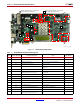
Chapter 1: AC701 Evaluation Board Features X-Ref Target - Figure 1-2 00 Round callout references a component on the front side of the board 00 Square callout references a component on the back side of the board 21 29 32 31 25 26 27 4 13 16 19 7 6 3 30 5 30 11 28 2 1 20 8 10 11 23 14 9 18 17 15 24 22 12 UG952_c1_02_011513 Figure 1-2: Table 1-1: AC701 Board Components AC701 Board Component Descriptions Callout Reference Designator Component Description Schematic 0381502 Page
Feature Descriptions Table 1-1: AC701 Board Component Descriptions (Cont’d) Callout Reference Designator Component Description Notes Schematic 0381502 Page Number 17 P2, U48 HDMI Video Connector and Device Molex 500254-1927, Analog Devices ADV7511KSTZ-P 19, 18 18 J23 LCD Character Display Connector 2 x 7 0.
Chapter 1: AC701 Evaluation Board Features X-Ref Target - Figure 1-3 FPGA_3V3 SW1 FPGA_M2 FPGA_M1 FPGA_M0 1 NC 2 3 6 5 4 SDA03H1SBD R339 1.21K 1% 1/10W R338 1.21K 1% 1/10W R337 1.21K 1% 1/10W UG952_c1_03_011713 Figure 1-3: SW1 Default Settings The default mode setting is M[2:0] = 001, which selects Master SPI at board power-on. Refer to the Configuration Options, page 75 for more information about the mode switch SW1.
Feature Descriptions X-Ref Target - Figure 1-4 NC 1 VCC1V8 (1.8V) D6 40V 200 mW 3 BAS40-04 1 FPGA_VBATT 2 2 R83 4.70K 5% 1/10W 1 B1 + 1.5V Seiko TS518SE_FL35E 2 GND UG952_c1_04_092812 Figure 1-4: Encryption Key Backup Circuit I/O Voltage Rails In addition to Bank 0, there are 8 I/O banks available on the Artix-7 device. The voltages applied to the FPGA I/O banks used by the AC701 board are listed in Table 1-3.
Chapter 1: AC701 Evaluation Board Features DDR3 Memory Module [Figure 1-2, callout 2] The memory module at J1 is a 1 GB DDR3 small outline dual-inline memory module (SODIMM). It provides volatile synchronous dynamic random access memory (SDRAM) for storing user code and data. The SODIMM socket has a perforated EMI shield surrounding it as seen in Figure 1-2. • Part number: MT8JTF12864HZ-1G6G1 (Micron Technology) • Supply voltage: 1.
Feature Descriptions Table 1-4: DDR3 Memory Connections to the FPGA (Cont’d) J1 DDR3 Memory U1 FPGA Pin AC701 Evaluation Board UG952 (v1.
Chapter 1: AC701 Evaluation Board Features Table 1-4: DDR3 Memory Connections to the FPGA (Cont’d) J1 DDR3 Memory U1 FPGA Pin 14 Net Name Pin Number Pin Name D1 DDR3_D33 131 DQ33 E1 DDR3_D34 141 DQ34 E2 DDR3_D35 143 DQ35 F2 DDR3_D36 130 DQ36 A2 DDR3_D37 132 DQ37 A3 DDR3_D38 140 DQ38 C2 DDR3_D39 142 DQ39 C3 DDR3_D40 147 DQ40 D3 DDR3_D41 149 DQ41 A4 DDR3_D42 157 DQ42 B4 DDR3_D43 159 DQ43 C4 DDR3_D44 146 DQ44 D4 DDR3_D45 148 DQ45 D5 DDR3_D46 158 DQ4
Feature Descriptions Table 1-4: DDR3 Memory Connections to the FPGA (Cont’d) J1 DDR3 Memory U1 FPGA Pin AC701 Evaluation Board UG952 (v1.
Chapter 1: AC701 Evaluation Board Features Table 1-4: DDR3 Memory Connections to the FPGA (Cont’d) J1 DDR3 Memory U1 FPGA Pin Net Name Pin Number Pin Name P1 DDR3_RAS_B 110 RAS_B P4 DDR3_CKE0 73 CKE0 N4 DDR3_CKE1 74 CKE1 L2 DDR3_CLK0_N 103 CK0_N M2 DDR3_CLK0_P 101 CK0_P N2 DDR3_CLK1_N 104 CK1_N N3 DDR3_CLK1_P 102 CK1_P The AC701 board DDR3 memory interface adheres to the constraints guidelines documented in the DDR3 Design Guidelines section of UG586, 7 Series FPGAs Memory
Feature Descriptions Flash memory on the AC701 board. For more details, see the Numonyx N25Q256A13ESF40G data sheet http://www.micron.com. X-Ref Target - Figure 1-5 VCC3V3 R20 DNP R19 4.7kΩ 5% R21 4.7kΩ 5% C18 0.1μF 25V X5R U7 N25Q256 256 Mb Serial Flash Memory GND FLASH_D3_R FLASH_D3 1 2 R429 15Ω 1% 3 4 QSPI_IC_CS_B FLASH_D1 VCC3V3 VCC3V3 R430 15Ω 1% C HOLD_B/DQ3 DQ0 VCC NC0 NC7 NC1 NC6 5 NC2 6 NC3 7 SB 8 FLASH_D2_R R17 DNP DQ1 R18 4.
Chapter 1: AC701 Evaluation Board Features X-Ref Target - Figure 1-6 J7 1 FPGA_PROG_B 2 FLASH_D3 3 FLASH_D2 4 QSPI_CS_B 5 FLASH_D0 6 7 8 9 FLASH_D1 HDR 1X9 Figure 1-6: VCC3V3 FPGA_CCLK GND UG952_c1_06_092812 SPI J7 External Programming Connector SD Card Interface [Figure 1-2, callout 4] The AC701 board includes a secure digital input/output (SDIO) interface to provide user-logic access to general purpose non-volatile SDIO memory cards and peripherals.
Feature Descriptions Table 1-7: SDIO Connections to the FPGA U29 SDIO Connector U1 FPGA Pin Name Schematic Net Name R20 AC701 Evaluation Board UG952 (v1.1) January 30, 2013 Pin Number Pin Name SDIO_SDWP 11 SDWP P24 SDIO_SDDET 10 SDDET N23 SDIO_CMD 2 CMD N24 SDIO_CLK 5 CLK P23 SDIO_DAT2 9 DAT2 N19 SDIO_DAT1 8 DAT1 P19 SDIO_DAT0 7 DAT0 P21 SDIO_CD_DAT3 1 CD_DAT3 www.xilinx.
Chapter 1: AC701 Evaluation Board Features USB JTAG Module [Figure 1-2, callout 5] JTAG configuration is provided through a Digilent onboard USB-to-JTAG configuration logic module (U26) where a host computer accesses the AC701 board JTAG chain through a standard-A plug (host side) to micro-B plug (AC701 board side) USB cable. A 2-mm JTAG header (J4) is also provided in parallel for access by Xilinx download cables such as the Platform Cable USB II and the Parallel Cable IV.
Feature Descriptions X-Ref Target - Figure 1-9 VCC3V3 VCC3V3 U26 Digilent USB-JTAG Module U19 J30 SN74LV541A Buffer FMC1_HPC_PRSNT_M2C_B R95 15Ω FMC_TDI_BUF TDI FMC1 HPC Connector PRSNT_L TDI U27 R96 15Ω TMS R94 15Ω FMC1_TDO_FPGA_TDI TCK FMC1_HPC_TMS_BUF FMC1_HPC_TCK_BUF TDO TDO TMS TCK VCC3V3 J4 JTAG Header U1 TDI TMS TCK TDO Artix-7 FPGA JTAG_TDI JTAG_TMS Bank 14 N16 JTAG_TCK JTAG_TDO Bank 0 FPGA_TDI_BUF FPGA_TCK_BUF FPGA_TMS_BUF FPGA_TDO TDI TCK TMS TDO UG952_c1_09_101512 Fi
Chapter 1: AC701 Evaluation Board Features System Clock Source [Figure 1-2, callout 6] The AC701 board has a 2.5V LVDS differential 200 MHz oscillator (U51) soldered onto the back side of the board and wired to an FPGA MRCC clock input on bank 34. This 200 MHz signal pair is named SYSCLK_P and SYSCLK_N, which are connected to FPGA U1 pins R3 and P3 respectively. • Oscillator: Si Time SiT9102AI-243N25E200.
Feature Descriptions Programmable User Clock Source [Figure 1-2, callout 7] The AC701 board has a programmable low-jitter 3.3V differential oscillator (U34) driving the FPGA MRCC inputs of bank 14. This USER_CLOCK_P and USER_CLOCK_N clock signal pair are connected to FPGA U1 pins M21 and M22 respectively. On power-up the user clock defaults to an output frequency of 156.250 MHz. User applications can change the output frequency within the range of 10 MHz to 810 MHz through an I2C interface.
Chapter 1: AC701 Evaluation Board Features User SMA Clock Input [Figure 1-2, callout 8] An external high-precision clock signal can be provided to the FPGA bank 15 by connecting differential clock signals through the onboard 50Ω SMA connectors J31 (P) and J32 (N). The differential clock signal names are USER_SMA_CLOCK_P and USER_SMA_CLOCK_N, which are connected to FPGA U1 pins J23 and H23 respectively. The user-provided differential clock circuit is shown in Figure 1-12.
Feature Descriptions GTP Clock MUX The AC701 board FPGA U1 MGT Bank 213 has two clock inputs, MGTREFCLK0 and MGTREFCLK1. Each clock input is driven by a capacitively-coupled clock sourced from a SY9544UMG 4-to-1 MUX. Each MUX has a clock source at three of its four inputs, the fourth input is not connected. Clock MUX U3 SY89544UMG drives Bank 213 MGTREFCLK0 pins AA13 (P) and AB13 (N), and clock MUX U4 SY89544UMG drives Bank 213 MGTREFCLK1 pins AA11 (P) and AB11 (N).
Chapter 1: AC701 Evaluation Board Features 125 MHz Clock Generator [Figure 1-2, callout 15] Clock MUX U3 input 0 (pin4 P, pin 2 N) is driven by U2 ICS84402I Crystal-to-LVDS clock generator. This device uses 25 MHz crystal X3 as its base input frequency and, via an internal VCO, multiplies this by five to produce a 0.45 ps (typical) RMS phase jitter, 125 MHz LVDS output. The circuit for the 125 MHz clock is shown in Figure 1-13.
Feature Descriptions Jitter Attenuated Clock [Figure 1-2, callout 10] The AC701 board includes a Silicon Labs Si5324 jitter attenuator U24 on the back side of the board. FPGA user logic can implement a clock recovery circuit and then output this clock to a differential I/O pair on I/O bank 16 (REC_CLOCK_C_P, FPGA U1 pin D23 and REC_CLOCK_C_N, FPGA U1 pin D24) for jitter attenuation. Duplicate capacitively coupled jitter attenuated clocks are routed to a pair of MGT clock MUXes U3 and U4.
Chapter 1: AC701 Evaluation Board Features FMC HPC GBT Clocks The FMC HPC connector J30 sources two MGT clocks, FMC1_HPC_GBTCLK0_M2C_P/N from connector section D, and FMC1_HPC_GBTCLK1_M2C_P/N from connector section B. Table 1-10 and Table 1-11 list the MGT clock MUX U3 and U4 connections.
Feature Descriptions X-Ref Target - Figure 1-16 VCC2V5 VCC2V5 U3 SY89544UMG 1 5 EPHYCLK_Q0_P VCC1 VCC3 VCC2 VCC4 4 IN0 NC EPHYCLK_Q0_N 3 VT0 2 IN0 SI5324_OUT0_C_P NC 31 VT1 30 IN1 VCC6 24 50 VCC7 28 VCC8 29 1 50 50 FMC1_HBC_GBTCLK0_M2C_C_P 27 IN2 NC 26 VT2 FMC1_HBC_GBTCLK0_M2C_C_N 25 IN2 2 NC 21 IN3 6 19 C320 0.1μF 25V X5R SFP_MGT_CLK0_P Q 11 SFP_MGT_CLK0_P GND2 9 50 GND Q 10 GND1 7 50 GND3 12 NC 23 IN3 NC 22 VT3 17 C105 0.
Chapter 1: AC701 Evaluation Board Features X-Ref Target - Figure 1-17 VCC2V5 VCC2V5 U4 SY89544UMG 1 5 SMA_MGT_REFCLK_P SI5324_OUT1_C_P VCC3 VCC2 VCC4 4 IN0 NC SMA_MGT_REFCLK_N VCC1 3 VT0 2 IN0 30 IN1 VCC6 24 50 VCC7 28 VCC8 29 1 50 50 FMC1_HBC_GBTCLK1_M2C_C_P 27 IN2 NC 26 VT2 FMC1_HBC_GBTCLK1_M2C_C_N 25 IN2 2 NC 21 IN3 6 19 C321 0.1μF 25V X5R SFP_MGT_CLK1_P Q 11 SFP_MGT_CLK1_P GND2 9 50 GND Q 10 GND1 7 50 GND3 12 NC 23 IN3 NC 22 VT3 17 C106 0.
Feature Descriptions GTP Transceivers [Figure 1-2, callout 11] The AC701 board provides access to 8 GTP transceivers: • Four of the GTP transceivers are wired to the PCI Express® x4 endpoint edge connector (P1) fingers • Two of the GTP transceivers are wired to the FMC HPC connector (J30) • One GTP is wired to SMA connectors (RX: J46, J47 TX: J44, J45) • One GTP is wired to the SFP/SFP+ Module connector (P3) The GTP transceivers in 7 series FPGAs are grouped into four channels described as Quads.
Chapter 1: AC701 Evaluation Board Features Table 1-12: GTP Interface Connections for FPGA U1 Transceiver Bank Placement GTP_BANK_213 GTPE2_CHANNEL_ X0Y0 GTPE2_CHANNEL_ X0Y1 GTPE2_CHANNEL_ X0Y2 GTPE2_CHANNEL_ X0Y3 GTPE2_CHANNEL_ X0Y0 32 Pin Number Pin Name Schematic Net Name Connected Connected Device Pin AC10 MGTPTXP0_213 SFP_TX_P P3.18 SFP+ Conn. P3 AD10 MGTPTXN0_213 SFP_TX_N P3.19 SFP+ Conn. P3 AC12 MGTPRXP0_213 SFP_RX_P P3.13 SFP+ Conn. P3 AD12 MGTPRXN0_213 SFP_RX_N P3.
Feature Descriptions Table 1-12: GTP Interface Connections for FPGA U1 (Cont’d) Transceiver Bank Placement GTP_BANK_216 GTPE2_CHANNEL_ X0Y4 GTPE2_CHANNEL_ X0Y5 GTPE2_CHANNEL_ X0Y6 GTPE2_CHANNEL_ X0Y7 GTPE2_CHANNEL_ X0Y1 Pin Number Pin Name Schematic Net Name Connected Connected Device Pin B7 MGTPTXP0_216 PCIE_TX3_P P1.A29(2) PCIe Edge Conn. P1 A7 MGTPTXN0_216 PCIE_TX3_N P1.A30(2) PCIe Edge Conn. P1 B11 MGTPRXP0_216 PCIE_RX3_P P1.B27 PCIe Edge Conn.
Chapter 1: AC701 Evaluation Board Features X-Ref Target - Figure 1-18 P1 PCI Express Four-Lane Edge connector A13 PCIE_CLK_Q0_C_P C188 0.01μF 25V X7R PCIE_CLK_Q0_P A14 PCIE_CLK_Q0_C_N PCIE_CLK_Q0_N OE GND REFCLK+ REFCLKGND A12 A15 C189 0.01μF 25V X7R GND UG952_c1_18_100312 Figure 1-18: PCI Express Clock PCIe lane width/size is selected via jumper J12 (Figure 1-19). The default lane size selection is 4-lane (J12 pins 3 and 4) jumpered).
Feature Descriptions X-Ref Target - Figure 1-20 VCC3V3 P3 VCC3V3 L6 4.7μH 3.0 A SFP+ Module Connector 74441-0010 L7 4.7μH 3.0 A SFP_VCCR 15 SFP_VCCT 16 C114 22μF 25V X5R C23 0.1μF 25V X5R C22 0.
Chapter 1: AC701 Evaluation Board Features Table 1-14 lists the SFP+ module control and status connections.
Feature Descriptions Table 1-15: Ethernet PHY U12 Configuration Pin Settings U12 Pin Name (No.
Chapter 1: AC701 Evaluation Board Features Ethernet PHY Clock Source A 25.00 MHz, 50 ppm crystal at X1 is the clock source for the 88E1116R PHY at U12. Figure 1-21 shows the clock source. X-Ref Target - Figure 1-21 C406 18pF 50V NPO X1 25.00 MHz 50 ppm R275 1.
Feature Descriptions Refer to the Marvell 88E1116R Alaska Gigabit Ethernet transceiver datasheet for details concerning the use of the Ethernet PHY user LEDs. They are referred to in the datasheet as LED0, LED1, and LED2. The product brief and other product information for the Marvell 88E1116R Alaska Gigabit ethernet transceiver is available at: http://www.marvell.
Chapter 1: AC701 Evaluation Board Features Table 1-18: FPGA to UART Connections U1 FPGA Pin UART function in FPGA Schematic Net Name U44 CP2103GM Pin UART Function in CP2103GM W19 RTS, output USB_UART_ CTS 22 CTS, input V19 CTS, input USB_UART_ RTS 23 RTS, output U19 TX, data out USB_UART_ RX 24 RXD, data in T19 RX, data in USB_UART_ TX 25 TXD, data out Refer to the Silicon Labs website for technical information on the CP2103GM and the VCP drivers http://www.silabs.com.
Feature Descriptions Figure 1-23 shows the HDMI codec circuit. X-Ref Target - Figure 1-23 VCC3V3 R104 2.43K 1/10W 1% 1 HDMI_INT VCC1V8 VCC2V5 U41 R106 2.43K 1/10W 1% R105 2.
Chapter 1: AC701 Evaluation Board Features Table 1-19 lists the connections between the codec and the FPGA.
Feature Descriptions Table 1-20 lists the connections between the codec and the HDMI connector P2.
Chapter 1: AC701 Evaluation Board Features X-Ref Target - Figure 1-25 FPGA_3V3 VCC5V0 C473 0.1μF 25V X5R U45 TXS0108E 8-Bit Bidirectional Voltage Level Translator GND LCD_E_LS LCD_RW_LS LCD_DB4_LS LCD_DB5_LS LCD_DB6_LS LCD_DB7_LS LCD_RS_LS C472 0.
Feature Descriptions Table 1-21 lists the connections between the FPGA and the LCD header. If the LCD is not installed, the J23 pins listed in Table 1-21 can be used for GPIO. Table 1-21: FPGA to LCD Header Connections FPGA Pin (U1) Schematic Net Name LCD Header Pin (J23) L25 LCD_DB4_LS 4 M24 LCD_DB5_LS 3 M25 LCD_DB6_LS 2 L22 LCD_DB7_LS 1 L24 LCD_RW_LS 10 L23 LCD_RS_LS 11 L20 LCD_E_LS 9 References The datasheet for the Displaytech S162DBABC LCD can be found at http://www.
Chapter 1: AC701 Evaluation Board Features . Table 1-22 lists the address for each bus.
Feature Descriptions Table 1-23: AC701 Board LEDs (Cont’d) Reference Designator Description Notes Schematic Page DS19 VCCO_VADJ ON Lumex SML-LX0603GW 46 DS20 DDR3 SODIMM RTERM VTT ON Lumex SML-LX0603GW 44 DS21 VCC3V3 ON Lumex SML-LX0603GW 48 DS22 12V INPUT POWER ON Lumex SML-LX0603GW 38 DS23 U9 TI Controller #2 PWRGOOD Lumex SML-LX0603GW 45 DS24 MGTAVCC ON Lumex SML-LX0603GW 49 DS25 MGTAVTT ON Lumex SML-LX0603GW 50 DS26 FPGA_1V8 ON Lumex SML-LX0603GW 47 DS27 DDR3 SODIM
Chapter 1: AC701 Evaluation Board Features User GPIO LEDs [Figure 1-2, callout 21] Figure 1-28 shows the user LED circuits. X-Ref Target - Figure 1-28 GPIO_LED_0 GPIO_LED_1 GPIO_LED_2 GPIO_LED_3 DS5 DS4 DS3 DS2 R150 49.9Ω 1% R149 49.9Ω 1% R148 49.9Ω 1% R147 49.9Ω 1% GND UG952_c1_28_100312 Figure 1-28: User LEDs User Pushbuttons and Reset Switch [Figure 1-2, callout 22] Figure 1-29 shows the user pushbutton switch circuits. X-Ref Target - Figure 1-29 FPGA_1V5 SW3 GPIO SW N 4 1 3 2 R36 4.
Feature Descriptions Figure 1-30 shows the user CPU_RESET pushbutton switch circuit. X-Ref Target - Figure 1-30 FPGA_1V5 SW8 CPU_RESET 4 1 3 2 R41 4.7kΩ 0.1 W 5% GND Figure 1-30: UG952_c1_140_011813 CPU_RESET Pushbutton GPIO DIP Switch [Figure 1-2, callout 23] Figure 1-31 shows the GPIO DIP Switch circuit. X-Ref Target - Figure 1-31 SW2 FPGA_1V5 GPIO_DIP_SW0 1 8 GPIO_DIP_SW1 GPIO_DIP_SW2 2 7 3 6 GPIO_DIP_SW3 4 5 R50 4.7kΩ 0.1 W 5% R52 4.7kΩ 0.1 W 5% R53 4.7kΩ 0.
Chapter 1: AC701 Evaluation Board Features User SMA Connectors [Figure 1-2, callout 25] Figure 1-33 shows the user SMA connector circuit. X-Ref Target - Figure 1-33 J33 SMA Connector USER_SMA_GPIO_P J34 GND SMA Connector USER_SMA_GPIO_N GND UG952_c1_142_011813 Figure 1-33: User SMA Connector LCD Connector Figure 1-34 shows the LCD J23 2x7 male pin header circuit.
Feature Descriptions Table 1-24 lists the GPIO Connections to FPGA U1. Table 1-24: GPIO Connections to FPGA U1 FPGA (U1) Pin Schematic Net Name GPIO Pin User LEDs (Active High) M26 GPIO_LED_0 DS2.2 T24 GPIO_LED_1 DS3.2 T25 GPIO_LED_2 DS4.2 R26 GPIO_LED_3 DS5.2 Directional Push-Button Switches (Active High) P6 GPIO_SW_N SW3.3 U5 GPIO_SW_E SW4.3 T5 GPIO_SW_S SW5.3 R5 GPIO_SW_W SW7.3 U6 GPIO_SW_C SW6.3 CPU_RESET Push-Button Switches (Active High) U4 CPU_RESET SW8.
Chapter 1: AC701 Evaluation Board Features Table 1-24: GPIO Connections to FPGA U1 (Cont’d) FPGA (U1) Pin Schematic Net Name GPIO Pin User LCD male pin header L22 LCD_DB7 J23.1 M25 LCD_DB6 J23.2 M24 LCD_DB5 J23.3 L25 LCD_DB4 J23.4 L20 LCD_E J23.9 L24 LCD_RW J23.10 L23 LCD_RS J23.11 User GPIO PMOD male pin header P26 PMOD_0 J48.1 T22 PMOD_1 J48.2 R22 PMOD_2 J48.3 T23 PMOD_3 J48.
Feature Descriptions Figure 1-36 shows the simplified diagram of the power connector J49, power switch SW15 and indicator LED DS22.
Chapter 1: AC701 Evaluation Board Features Configuration Mode Switch SW1 The AC701 board supports two of the five 7 series FPGA configuration modes: • Master SPI using the on-board Quad SPI flash memory • JTAG using a standard-A to micro-B USB cable for connecting the host PC to the AC701 board configuration port (via Digilent module) Each configuration interface corresponds to one or more configuration modes and bus widths as listed in Table 1-25.
Feature Descriptions The Samtec connector system is rated for signaling speeds up to 9 GHz (18 Gb/s) based on a -3 dB insertion loss point within a two-level signaling environment. Connector Type: • Samtec SEAF Series, 1.27 mm (0.050 in) pitch. Mates with SEAM series connector For more information about SEAF series connectors, go to the Samtec website at: www.samtec.com.
Chapter 1: AC701 Evaluation Board Features Table 1-26: HPC Connections, J30 to FPGA U1 (Cont’d) J30 FMC HPC Pin 56 Schematic Net Name U1 FPGA J30 FMC Pin HPC Pin Schematic Net Name U1 FPGA Pin A19 NC NA B20 FMC1_HPC_GBTCLK1_M2C_P U4.27 A22 FMC1_HPC_DP1_C2M_P AC8 B21 FMC1_HPC_GBTCLK1_M2C_N U4.
Feature Descriptions Table 1-26: HPC Connections, J30 to FPGA U1 (Cont’d) J30 FMC HPC Pin Schematic Net Name U1 FPGA J30 FMC Pin HPC Pin Schematic Net Name U1 FPGA Pin D33 FMC1_HPC_TMS_BUF U19.
Chapter 1: AC701 Evaluation Board Features Table 1-26: HPC Connections, J30 to FPGA U1 (Cont’d) J30 FMC HPC Pin 58 Schematic Net Name U1 FPGA J30 FMC Pin HPC Pin Schematic Net Name U1 FPGA Pin G2 FMC1_HPC_CLK1_M2C_P H1 NC NA G3 FMC1_HPC_CLK1_M2C_N H2 FMC1_HPC_PRSNT_M2C N16 G6 FMC1_HPC_LA00_CC_P D18 H4 FMC1_HPC_CLK0_M2C_P D19 G7 FMC1_HPC_LA00_CC_N C18 H5 FMC1_HPC_CLK0_M2C_N C19 G9 FMC1_HPC_LA03_P G17 H7 FMC1_HPC_LA02_P H14 G10 FMC1_HPC_LA03_N F17 H8 FMC1_HPC_LA02_N H
Feature Descriptions Table 1-26: HPC Connections, J30 to FPGA U1 (Cont’d) J30 FMC HPC Pin Schematic Net Name U1 FPGA J30 FMC Pin HPC Pin Schematic Net Name U1 FPGA Pin J10 FMC1_HPC_HA07_N AD24 K10 FMC1_HPC_HA06_P AE23 J12 FMC1_HPC_HA11_P AD20 K11 FMC1_HPC_HA06_N AF23 J13 FMC1_HPC_HA11_N AE20 K13 FMC1_HPC_HA10_P AE22 J15 FMC1_HPC_HA14_P AE18 K14 FMC1_HPC_HA10_N AF22 J16 FMC1_HPC_HA14_N AF18 K16 FMC1_HPC_HA17_CC_P AA20 J18 FMC1_HPC_HA18_P AA17 K17 FMC1_HPC_HA17_CC_N
Chapter 1: AC701 Evaluation Board Features The UCD90120A device is configured by using the PC-based TI Fusion Digital Power Designer software. This software provides a graphical user interface (GUI) for configuring, storing, and monitoring power system operating parameters.
Feature Descriptions Figure 1-40 shows the power system for UCD90120A U8 controller #1 X-Ref Target - Figure 1-40 U49 (1.0V Nom) U8 UCD90120A Controller (Controller 1) GPIO (Out) FPWM (Out) ADC (In) ADC (In) GPIO (Out) +12V LMZ12008 Vin Vout Input Filter VCCINT 1.0V Cf(1) Cf Rail Enable V fb PWM Margin Rs 5mΩ EN FB G = 40.22 VCCINT 0A-10A CS = 0V-2.01V Current Sense Voltage Sense(2) Low Pwr Select U53 (1.
Chapter 1: AC701 Evaluation Board Features Table 1-28 shows the AC701 TI power system configuration for controller U9. Table 1-28: Controller U9 Power System Configuration Schematic Sequencer Regulator Type Voltage Current VCCO_VADJ TPS84621 (U56) 2.5V 6A Addr 102, Rail 2 FPGA_1V8 TPS84320 (U57) 1.8V 3A 48 Addr 102, Rail 3 FPGA_3V3 TPS84621 (U58) 3.3V 6A 49 Addr 102, Rail 4 MGTAVCC TPS84320 (U59) 1.0V 3A 50 Addr 102, Rail 5 MGTAVTT TPS84320 (U60) 1.
Feature Descriptions Figure 1-41 shows the power system for UCD90120A U9 controller #2 rails 1 through 5. X-Ref Target - Figure 1-41 U9 UCD90120A Controller (Controller 2) GPIO (Out) FPWM (Out) ADC (In) ADC (In) GPIO (Out) Notes: 1. Capacitors labled Cf are bulk filter capacitors. 2. Voltage Sense is connected +12V at point of load. U49 (2.
Chapter 1: AC701 Evaluation Board Features The TPS84K and LMZ22000 family adjustable voltage regulators have their output voltage set by an external resistor. The regulator topology on the AC701 board permits the UCD90120A to monitor rail voltage and current. Voltage margining at +5% and -5% is also implemented. Each voltage regulator's external VOUT setting resistor is calculated and implemented as if the regulator is standalone.
Feature Descriptions Figure 1-42 shows the XADC external multiplexer block diagram. X-Ref Target - Figure 1-42 FPGA_1V5_SENSE_P 1.00 K FPGA_1V5_XADC_P (1.5V Scaled to 0.75V) 1.00 K FPGA_1V5_XADC_N GND VCCO_VADJ_SENSE_P U14 3.01 K ADG707BRU VCCINT_XADC_CS_P/N S1A/B VCCAUX_XADC_CS_P/N S2A/B VCCBRAM_XADC_CS_P/N S3A/B DA U1 FPGA_1V5_XADC_P/N S4A/B DB FPGA_1V5_XADC_CS_P/N S5A/B XC7A200T FPGA (Bank 15) 49.9 ADIP K16 A[2:0] 1.
Chapter 1: AC701 Evaluation Board Features See Tables Table 1-29 and Table 1-30 which list the AC701 board XADC power system voltage and current measurement details for the external muxes U14 and U13. Table 1-29: XADC Measurements through Mux U14 Isense Op Amp Measurement Type Rail Name Current Range V VCCINT I VCCINT CS 8-to-1 Multiplexer U14 Reference Designator Gain Vo Range NA NA NA NA 0A-4A U16 50 0V-0.996V V VCCAUX NA NA NA NA I VCCAUX CS 0A-6A U17 30 0V-0.
Feature Descriptions Table 1-30: XADC Measurements through Mux U13 (Cont’d) Isense Op Amp Measurement Type Rail Name Current Range V MGTAVTT SENSE NA MGTAVTT CS 0A-1.5A I Reference Designator Gain 8-to-1 Multiplexer U14 100 Pin Number Pin Name MGTAVTT_XADC_P 24 S6A MGTAVTT_SENSE_N 6 S6B MGTAVTT_XADC_CS_P 25 S7A MGTAVTT_XADC_CS_N 5 S7B NC 26 S8A NC 4 S8B Vo Range MGTAVTT REMOTE SENSE DIVIDED TO DELIVER 0.
Chapter 1: AC701 Evaluation Board Features X-Ref Target - Figure 1-43 J49 12V PWR Jack Power Controller 1 PMBUS 101 U8 Switching Regulator 1.0V at 8A U49 VCCINT Switching Module 1.8V at 3A U53 VCCAUX Switching Module 1.0V at 3A U54 VCCBRAM Switching Module 1.5V at 6A U55 FPGA_1V5 U9 Power Controller 2 PMBUS 102 Switching Module 1.2V–3.3V at 6A U56 VCCO_VAJ Switching Module 1.8V at 6A U57 FPGA_1V8 Switching Module 3.3V at 6A U58 VCC3V3 Switching Module 1.
Feature Descriptions The AC701 board core and auxiliary voltages are listed in Table 1-25. Table 1-31: AC701 Board Onboard Power System Devices Power Rail Net Name Power Rail Voltage Schematic Page Reference Designator Description UCD90120A (4 Rails) U8 PMBus Controller - PMBus Addr = 101 LMZ22010TZ U49 10A 0.8V - 6V Adj. Switching Regulator VCCINT 1.00V 40 TPS84621RUQ U53 6A 0.6V - 5.5V Adj. Switching Regulator VCCAUX 1.80V 41 TPS84320RUQ U54 3A 0.6V - 5.5V Adj.
Chapter 1: AC701 Evaluation Board Features internally ORs these PG conditions together and drives an output PG pin high only if all active rail PG states are good. The on and off delay parameter values are relative to when the board power on-off slide switch SW15 is turned on and off. Table 1-32 defines the voltage and current values for each power rail controlled by the UCD90120A U8 controller at PMBus Address 101.
Feature Descriptions In this VCCO_VADJ off mode, the user can control when to turn on VCCO_VADJ and to what voltage level (1.8V, 2.5V or 3.3V). With VCCO_VADJ off, the FPGA still configures and has access to the TI controller PMBUS and the VADJ_ON_B signal which are wired to FPGA U1 Bank 14. The combination of these features allows the user to develop code to command the VCCO_VADJ rail to be set to 1.8V or 3.3V instead of the default setting of 2.5V.
Chapter 1: AC701 Evaluation Board Features X-Ref Target - Figure 1-44 VCC12_P R245 10.0K 1% 1/10W J61 Fan Tach Cooling Fan Fan +12V Fan GND 3 R393 10.0K 1% 1/10W 2 D14 100V 500 mW DL4148 1 VCC2V5 FPGA U1 Pin J26 SM_FAN_PWM 2 R277 1.00K 1% 1/16W 1 SM_FAN_TACH R390 4.75K 1% 1/10W FPGA U1 Pin J25 D15 2.7V 500 mW MM3Z2V7B GND 4 Q17 NDT30555L 1.
Feature Descriptions X-Ref Target - Figure 1-45 VCCAUX Ferrite Bead XADC_VCC U1 J43 FPGA XADC_VCC Header J49 1.8V 150 mV max XADC_VCC VCCADC XADC_VCC5V0 to XADC Header J19.13 Ferrite Bead U10 100 nF Close to Package Pins 10 μF XADC_AGND ADP123 In Out Gnd VCC5V0 J53 10 μF 100 nF 1 nF GNDADC XADC_AGND XADC_AGND Filter 5V Supply Locate Components on Board XADC_VREF to XADC Header J19.11 U35 VREF (1.
Chapter 1: AC701 Evaluation Board Features X-Ref Target - Figure 1-46 XADC_VN XADC_VAUX0P XADC_VCC5V0 VCCO_VADJ 1 3 5 7 9 11 13 15 17 19 XADC_VAUX8N XADC_DXP XADC_VREF XADC_GPIO_1 XADC_GPIO_3 J19 XADC_VP 2 4 6 8 10 12 14 16 18 20 XADC_VAUX0N XADC_VAUX8P XADC_DXN XADC_VCC_HEADER XADC_GPIO_0 XADC_GPIO_2 GND XADC_AGND XADC_AGND UG952_c1_40_101612 Figure 1-46: XADC header (J19) Table 1-35 describes the XADC header J19 pin functions.
Configuration Options Configuration Options The FPGA on the AC701 board can be configured using these methods: • Master SPI (uses the Quad-SPI Flash U7). • JTAG (uses the U26 Digilent USB-to-JTAG Bridge or J4 Download Cable connector). See USB JTAG Module, page 20 for more information. SeeUG480, 7 Series FPGAs XADC Dual 12-Bit 1MSPS Analog-to-Digital Converter User Guide for further details on configuration modes.
Chapter 1: AC701 Evaluation Board Features Figure 1-48 shows the QSPI U7 configuration circuit. X-Ref Target - Figure 1-48 U1 SW9 PROG_B FPGA VCC1V8 PROG_B SW1 GND Mode Switch M[2:0] Bank 0 VBATT TCK TMS TDI TDO D6 BAS40-04 VCC3V3 DONE DS10 GREEN D[3:0] U7 FCS_B B1 R396 261Ω CCLK N25Q256A13ESF40G QUAD SPI DQ[1:0] R396 4.7K GND Bank 14 GND DQ2_WP DQ3_HOLD_B U40 Oscillator 90 MHz C EMCCLK S-B SIT8103 UG952_c1_42_101612 Figure 1-48: 76 AC701 Board QSPI Configuration Circuit www.
Appendix A Default Switch and Jumper Settings User GPIO DIP Switch SW2 See Figure 1-2, page 8 callout 23 for location of SW2. Default settings are shown in Figure A-1 and details are listed in Table A-1. X-Ref Target - Figure A-1 ON Position = 1 1 2 3 4 SW2 OFF Position = 0 UG952_aA_01_100712 Figure A-1: Table A-1: AC701 Evaluation Board UG952 (v1.
Appendix A: Default Switch and Jumper Settings Configuration DIP Switch SW1 See Figure 1-2, page 8 callout 28 for location of SW1. Default settings are shown in Figure A-2 and details are listed in Table A-2. X-Ref Target - Figure A-2 ON Position = 1 3 M0 1 ON M2 2 M1 SW1 OFF Position = 0 UG952_aA_02_011813 Figure A-2: SW1 Default Settings The default mode setting M[2:0] = 001 selects Master SPI configuration at board power-on.
Default Jumper Settings Default Jumper Settings The AC701 board default jumper configurations are listed in Table A-3. Table A-3: Header AC701 Default Jumper Settings Jumper Description Schematic Page 2-pin J11 1-2 XADC VCCINT 4A range 34 J53 1-2 XADC_VCC5V0 = 5V 29 J9 1-2 REF3012 XADC_AGND L3 bypassed 29 J10 1-2 REF3012 XADC_AGND = GND 29 J63 None Voltage Regulators Enabled 38 J52 None Test Header, Not a Jumper 7 J5 1-2 EPHY U12.
Appendix A: Default Switch and Jumper Settings 80 www.xilinx.com AC701 Evaluation Board UG952 (v1.
Appendix B VITA 57.1 FMC Connector Pinouts Figure B-1 shows the pinout of the FPGA mezzanine card (FMC) high pin count (HPC) connector defined by the VITA 57.1 FMC specification. For a description of how the AC701 board implements the FMC specification, see FPGA Mezzanine Card Interface, page 54 and HPC Connector J30, page 55.
Appendix B: VITA 57.1 FMC Connector Pinouts 82 www.xilinx.com AC701 Evaluation Board UG952 (v1.
Appendix C Master Constraints File Listing TheAC701 board master Xilinx® design constraints (XDC) file template provides for designs targeting the AC701 board. Net names in the constraints listed in the AC701 Board XDC File Listing correlate with net names on the AC701 board schematic. Users must identify the appropriate pins and replace the net names in this list with net names in the user RTL. For more information, see UG903, Vivado Design Suite User Guide, Using Constraints: http://www.xilinx.
Appendix C: Master Constraints File Listing set_property set_property set_property set_property set_property set_property set_property set_property set_property set_property set_property set_property set_property set_property set_property set_property set_property set_property set_property set_property set_property set_property set_property set_property set_property set_property set_property set_property set_property set_property set_property set_property set_property set_property set_property set_property
AC701 Board XDC File Listing set_property set_property set_property set_property set_property set_property set_property set_property set_property set_property set_property set_property set_property set_property set_property set_property set_property set_property set_property set_property set_property set_property set_property set_property set_property set_property set_property set_property set_property set_property set_property set_property set_property set_property set_property set_property set_property s
Appendix C: Master Constraints File Listing set_property set_property set_property set_property set_property set_property set_property set_property set_property set_property set_property set_property set_property set_property set_property set_property set_property set_property set_property set_property set_property set_property set_property set_property set_property set_property set_property set_property set_property set_property set_property set_property set_property set_property set_property set_property
AC701 Board XDC File Listing set_property set_property set_property set_property set_property set_property set_property set_property set_property set_property set_property set_property set_property set_property set_property set_property set_property set_property set_property set_property set_property set_property set_property set_property set_property set_property set_property set_property set_property set_property set_property set_property AC701 Evaluation Board UG952 (v1.
Appendix C: Master Constraints File Listing 98 www.xilinx.com AC701 Evaluation Board UG952 (v1.
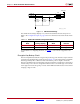
Appendix D Board Setup Installing the AC701 Board in a PC Chassis Installation of the AC701 board inside a computer chassis is required when developing or testing PCI Express functionality. When the AC701 board is used inside a computer chassis (i.e., plugged in to the PCIe® slot), power is provided from the ATX power supply 4-pin peripheral connector through the ATX adapter cable shown in Figure D-1 to J49 on the AC701 board. The Xilinx part number for this cable is 2600304.
Appendix D: Board Setup 8. 100 Slide the AC701 board power switch SW15 to the ON position. The PC can now be powered on. www.xilinx.com AC701 Evaluation Board UG952 (v1.
Appendix E Board Specifications Dimensions Height 5.5 in (14.0 cm) Length 10.5 in (26.7 cm) Note: The AC701 board height exceeds the standard 4.376 in (11.15 cm) height of a PCI Express card. Environmental Temperature Operating: 0°C to +45°C Storage: –25°C to +60°C Humidity 10% to 90% non-condensing Operating Voltage +12 VDC AC701 Evaluation Board UG952 (v1.1) January 30, 2013 www.xilinx.
Appendix E: Board Specifications 102 www.xilinx.com AC701 Evaluation Board UG952 (v1.
Appendix F Additional Resources Xilinx Resources For support resources such as Answers, Documentation, Downloads, and Forums, see the Xilinx Support website at: http://www.xilinx.com/support. Create a Xilinx user account and sign up to receive automatic e-mail notification whenever this document is updated: http://www.xilinx.com/support/myalerts. For a glossary of technical terms used in Xilinx documentation, see: www.xilinx.com/company/terms.htm.
Appendix F: Additional Resources UG475, 7 Series FPGAs Packaging and Pinout User Guide UG476, 7 Series FPGAs GTX Transceivers User Guide UG477 7 Series FPGAs Integrated Block for PCI Express User Guide UG480, 7 Series FPGAs XADC Dual 12-Bit 1MSPS Analog-to-Digital Converter User Guide UG483, 7 Series FPGAs PCB Design and Pin Planning Guide XTP230, AC701 Si570 Programming XTP229, AC701 Si570 Fixed Frequencies References Documents associated with other devices used by the AC701 board are available at these
Appendix G Regulatory and Compliance Information This product is designed and tested to conform to the European Union directives and standards described in this section. Refer to the AC701 board master answer record concerning the CE requirements for the PC Test Environment: http://www.xilinx.com/support/answers/51900.htm Declaration of Conformity To view the declaration of conformity online, visit: http://www.xilinx.com/support/documentation/boards_and_kits/ ce-declarations-of-conformity-xtp251.
Appendix G: Regulatory and Compliance Information EN 60950-1:2006, Information technology equipment – Safety, Part 1: General requirements Markings This product complies with Directive 2002/96/EC on waste electrical and electronic equipment (WEEE). The affixed product label indicates that the user must not discard this electrical or electronic product in domestic household waste.
IMPORTANT NOTICE FOR TI REFERENCE DESIGNS Texas Instruments Incorporated ("TI") reference designs are solely intended to assist designers (“Buyers”) who are developing systems that incorporate TI semiconductor products (also referred to herein as “components”). Buyer understands and agrees that Buyer remains responsible for using its independent analysis, evaluation and judgment in designing Buyer’s systems and products.