
User guide


AC701 Evaluation Board www.xilinx.com 33
UG952 (v1.1) January 30, 2013
Feature Descriptions
For more information on the GTP transceivers see UG476, 7 Series FPGAs GTX Transceivers
User Guide.
PCI Express Edge Connector
[Figure 1-2, callout 12]
The 4-lane PCI Express edge connector performs data transfers at the rate of 2.5 GT/s for a
Gen1 application and 5.0
GT/s for a Gen2 application. The PCIe transmit and receive
signal data paths have a characteristic impedance of 85Ω ±10%. The PCIe clock is routed as
a 100Ω differential pair. The 7
series FPGAs GTP transceivers are used for multi-gigabit per
second serial interfaces.
The XC7A200T-2FBG676C FPGA (-2 speed grade) included with the AC701 board
supports up to Gen2 x4.
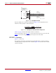
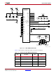
The PCIe clock is input from the edge connector. It is AC coupled to the FPGA through the
MGTREFCLK0 pins of Quad 216. PCIE_CLK_Q0_P is connected to FPGA U1 pin F11, and
the _N net is connected to pin E11. The PCI Express clock circuit is shown in
Figure 1-18.
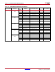
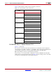
GTP_BANK_216 GTPE2_CHANNEL_
X0Y4
B7 MGTPTXP0_216 PCIE_TX3_P P1.A29
(2)
PCIe Edge Conn. P1
A7 MGTPTXN0_216 PCIE_TX3_N P1.A30
(2)
PCIe Edge Conn. P1
B11 MGTPRXP0_216 PCIE_RX3_P P1.B27 PCIe Edge Conn. P1
A11 MGTPRXN0_216 PCIE_RX3_N P1.B28 PCIe Edge Conn. P1
GTPE2_CHANNEL_
X0Y5
D8 MGTPTXP1_216 PCIE_TX2_P P1.A25
(2)
PCIe Edge Conn. P1
C8 MGTPTXN1_216 PCIE_TX2_N P1.A26
(2)
PCIe Edge Conn. P1
D14 MGTPRXP1_216 PCIE_RX2_P P1.B23 PCIe Edge Conn. P1
C14 MGTPRXN1_216 PCIE_RX2_N P1.B24 PCIe Edge Conn. P1
GTPE2_CHANNEL_
X0Y6
B9 MGTPTXP2_216 PCIE_TX1_P P1.A21
(2)
PCIe Edge Conn. P1
A9 MGTPTXN2_216 PCIE_TX1_N P1.A22
(2)
PCIe Edge Conn. P1
B13 MGTPRXP2_216 PCIE_RX1_P P1.B19 PCIe Edge Conn. P1
A13 MGTPRXN2_216 PCIE_RX1_N P1.B20 PCIe Edge Conn. P1
GTPE2_CHANNEL_
X0Y7
D10 MGTPTXP3_216 PCIE_TX0_P P1.A16
(2)
PCIe Edge Conn. P1
C10 MGTPTXN3_216 PCIE_TX0_N P1.A17
(2)
PCIe Edge Conn. P1
D12 MGTPRXP3_216 PCIE_RX0_P P1.B14 PCIe Edge Conn. P1
C12 MGTPRXN3_216 PCIE_RX0_N P1.B15 PCIe Edge Conn. P1
GTPE2_CHANNEL_
X0Y1
F11 MGTREFCLK0P_216 PCIE_CLK_QO_P P1.A13
(2)
PCIe Edge Conn. P1
E11 MGTREFCLK0N_216 PCIE_CLK_QO_N P1.A14
(2)
PCIe Edge Conn. P1
F13 MGTREFCLK1P_216 NC NA NA
E13 MGTREFCLK1N_216 NC NA NA
Notes:
1. Clock Mux U3 and U4 output nets are capacitively coupled to the GTP REFCLK input pins.
2. PCIE_TXn_P/N and PCIE_CLK_Q0_P/N are capacitively coupled to the PCIe edge connector P1.
Table 1-12: GTP Interface Connections for FPGA U1 (Cont’d)
Transceiver Bank Placement
Pin
Number
Pin Name Schematic Net Name
Connected
Pin
Connected Device