
User guide

70 www.xilinx.com AC701 Evaluation Board
UG952 (v1.1) January 30, 2013
Chapter 1: AC701 Evaluation Board Features
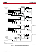
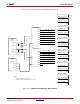
internally ORs these PG conditions together and drives an output PG pin high only if all
active rail PG states are good. The on and off delay parameter values are relative to when
the board power on-off slide switch SW15 is turned on and off.
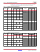
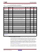
Table 1-32 defines the voltage and current values for each power rail controlled by the
UCD90120A U8 controller at PMBus Address 101.
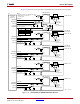
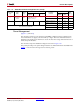
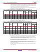
Table 1-33 defines the voltage and current values for each power rail controlled by the
UCD90120A U9 controller at PMBus Address 102.
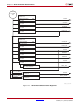
VCCO_VADJ Voltage Control
The FMC VCCO_VADJ rail is set to 2.5V. When the AC701 board is powered on, the state
of the FMC_VADJ_ON_B signal wired to header J8 is sampled by the TI UCD90120A
controller U9. If a jumper is installed on J8, signal FMC_VADJ_ON_B is held low, and TI
controller U9 energizes the FMC VCCO_VADJ rail at power on.
Removing the jumper at J8 after the board is powered up will not affect the 2.5V power
delivered to the VCCO_VADJ rail and it will remain on.
A jumper installed at J8 is the default setting. If a jumper is not installed on J8 at power-on,
the signal FMC_VADJ_ON_B is high and the AC701 board will not energize the
VCCO_VADJ 2.5V power.
Installing a jumper at J8 after the AC701 board powers up in this mode will turn on the
VCCO_VADJ rail.
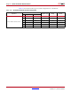
Table 1-32: Power Rail Specifications for UCD90120A PMBus Controller U8 at Address 101
Rail
Nominal
Voltage
Power Good On Power Good Off
Turn On
Delay
(ms)
Turn
Off
Delay
(ms)
Fault
Shutdown
Slaves
Rail Turn-on
Dependencies
Rail GPI
1 VINT_1V0 1.000 0.900 -10.0% 0.850 -15.0% 0.0 15.0 Rail #2,3,4 None None
2 VAUX_1V8 1.800 1.620 -10.0% 1.530 -15.0% 10.0 5.0 Rail #1,3,4 Rail #3 None
3 VBRAM_1V0 1.000 0.900 -10.0% 0.850 -15.0% 5.0 10.0 Rail #1,2,4 Rail #1 None
4 FPGA_1V5 1.500 1.350 -10.0% 1.275 -15.0% 15.0 0.0 Rail #1,2,3 Rail #2 None
Table 1-33: Power Rail Specifications for UCD90120A PMBus controller U9 at Address 102
Rail
Nominal
Voltage
Power Good On Power Good Off
Turn
On
Delay
(ms)
Turn
Off
Delay
(ms)
Fault
Shutdown
Slaves
Rail Turn-on
Dependencies
Rail GPI
1 VADJ_2V5 2.500 2.250 -10.0% 2.125 -15.0% 5.0 15.0 Rail #2,3,4,5 Rail #3
FMC_
VADJ _
ON_B
2 FPGA_1V8 1.800 1.620 -10.0% 1.530 -15.0% 10.0 10.0 Rail #1,3,4,5 None None
3 FPGA_3V3 3.300 2.970 -10.0% 2.805 -15.0% 0.0 20.0 Rail #1,2,4,5 None None
4 MGTVC_1V0 1.000 0.900 -10.0% 0.850 -15.0% 5.0 5.0 Rail #1,2,3,5 Rail #2 None
5 MGTVT_1V2 1.200 1.080 -10.0% 1.020 -15.0% 10.0 0.0 Rail #1,2,3,4 Rail #4 None