
- Silicon Laboratories, Inc. Clock User Manual

Si53xx-RM
18 Rev. 0.5
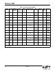
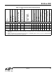
3.2. Si5319
The Si5319 is a jitter-attenuating precision M/N clock multiplier for applications requiring sub 1 ps jitter
performance. The Si5319 accepts one clock input ranging from 2 kHz to 710 MHz and generates one clock output
ranging from 2 kHz to 945 MHz and select frequencies to 1.4 GHz. The Si5319 can also use its crystal oscillator as
a clock source for frequency synthesis. The device provides virtually any frequency translation combination across
this operating range. The Si5319 input clock frequency and clock multiplication ratio are programmable through an
I2C or SPI interface. The Si5319 is based on Silicon Laboratories' 3rd-generation DSPLL
®
technology, which
provides any-frequency synthesis and jitter attenuation in a highly integrated PLL solution that eliminates the need
for external VCXO and loop filter components. The DSPLL loop bandwidth is digitally programmable, providing
jitter performance optimization at the application level. Operating from a single 1.8, 2.5, or 3.3 V supply, the Si5319
is ideal for providing clock multiplication and jitter attenuation in high performance timing applications. See "7.
Microprocessor Controlled Parts (Si5319, Si5324, Si5325, Si5326, Si5327, Si5367, Si5368, Si5369, Si5374,
Si5375)" on page 76 for a complete description.
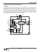
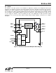
Figure 2. Si5319 Any-Frequency Jitter Attenuating Clock Multiplier Block Diagram
DSPLL
®
Loss of Signal
Xtal or Refclock
CKIN
CKOUT
÷ N31
÷ N2
Signal Detect
Device Interrupt
VDD
GND
Loss of Lock
Xtal/Clock Select
I
2
C/SPI Port
Control
Rate Select
÷ N32
XO
f
3
÷ N1_HS ÷ NC1